High voltage tolerance and quick charging/discharging characteristics are required for this product.
The products are used for snubber circuits, camera strobe circuits and Ethernet LAN(IEEE 802.3)They are also used in high-voltage environments.
General Features
Series(Floating) & Shield Design
Rated voltage 250V~3kV, Temperature Range -55℃ to +125℃, Case Size 0805 to 1812
Application
Switching Power Circuit(SMPS)
Lighting Ballast, LCD Back Lighting Inverter
DC-DC converter input filter, Snubber Circuit
Phone, Fax, Modem
Network(IEEE802.3)
Why Samsung
Features of products (technology)
Fail Safe Design
Optimized design through electrical / Mechanical Simulation
Series & Shield design (X7R : 500V~3kV, C0G : 1kV~3kV)
Series structure is an effective method that prevents short-mode failure. Shield structure prevents electric field concentration between inner and outer electrodes.
Open mode design (X7R, C0G : 1kV~3kV)
Open mode design prevents short-mode failure : L margin ≥ Bandwidth
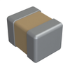
Sectional View
Realizes capacitance by layering dielectrics and internal electrodes.
※ May be divided into normal type and series type according to the layered structure.
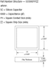
Size (inch)
Dimension(mm)
Length(L)
Width(W)
Thickness(T)
Thickness code
Band Width(BW)
0603
1.60±0.10
0.80±0.10
0.80±0.10
8
0.30±0.20
0805
2.00±0.10
1.25±0.10
0.65±0.10
A
0.50+0.20/-0.30
2.00±0.10
1.25±0.10
0.85±0.10
C
2.00±0.10
1.25±0.10
1.25±0.10
F
1206
3.20±0.15
1.60±0.15
0.85±0.15
C
0.50±0.30
3.20±0.15
1.60±0.15
1.25±0.15
F
3.20±0.20
1.60±0.20
1.60±0.20
H
1210
3.20±0.30
2.50±0.20
1.25±0.20
F
0.60±0.30
3.20±0.30
2.50±0.20
1.60±0.20
H
3.20±0.30
2.50±0.20
2.00±0.20
I
3.20±0.30
2.50±0.20
2.50±0.20
J
1808
4.50±0.40
2.00±0.20
1.25±0.20
F
0.80±0.30
4.50±0.40
2.00±0.20
1.60±0.20
H
4.50±0.40
2.00±0.20
2.00±0.20
I
1812
4.50±0.40
3.20±0.30
1.25±0.20
F
0.80±0.30
4.50±0.40
3.20±0.30
1.60±0.20
H
4.50±0.40
3.20±0.30
2.00±0.20
I
4.50±0.40
3.20±0.30
2.50±0.20
J
High voltage tolerance and quick charging/discharging characteristics are required for this product.
The products are used for snubber circuits, camera strobe circuits and Ethernet LAN(IEEE 802.3)They are also used in high-voltage environments.
General Features
- Series(Floating) & Shield Design
- Rated voltage 250V~3kV, Temperature Range -55℃ to +125℃, Case Size 0805 to 1812
Application
- Switching Power Circuit(SMPS)
- Lighting Ballast, LCD Back Lighting Inverter
- DC-DC converter input filter, Snubber Circuit
- Phone, Fax, Modem
- Network(IEEE802.3)
Why Samsung
Features of products (technology)
Fail Safe Design
- Optimized design through electrical / Mechanical Simulation
Series & Shield design (X7R : 500V~3kV, C0G : 1kV~3kV)
Series structure is an effective method that prevents short-mode failure.
Shield structure prevents electric field concentration between inner and outer electrodes.
Open mode design (X7R, C0G : 1kV~3kV)
Open mode design prevents short-mode failure :
L margin ≥ Bandwidth
Sectional View
Realizes capacitance by layering dielectrics and internal electrodes.
※ May be divided into normal type and series type according to the layered structure.
| Size (inch) | Dimension(mm) |
|---|
| Length(L) | Width(W) | Thickness(T) | Thickness code | Band Width(BW) |
|---|
| 0603 | 1.60±0.10 | 0.80±0.10 | 0.80±0.10 | 8 | 0.30±0.20 |
|---|
| 0805 | 2.00±0.10 | 1.25±0.10 | 0.65±0.10 | A | 0.50+0.20/-0.30 |
|---|
| 2.00±0.10 | 1.25±0.10 | 0.85±0.10 | C |
| 2.00±0.10 | 1.25±0.10 | 1.25±0.10 | F |
| 1206 | 3.20±0.15 | 1.60±0.15 | 0.85±0.15 | C | 0.50±0.30 |
|---|
| 3.20±0.15 | 1.60±0.15 | 1.25±0.15 | F |
| 3.20±0.20 | 1.60±0.20 | 1.60±0.20 | H |
| 1210 | 3.20±0.30 | 2.50±0.20 | 1.25±0.20 | F | 0.60±0.30 |
|---|
| 3.20±0.30 | 2.50±0.20 | 1.60±0.20 | H |
| 3.20±0.30 | 2.50±0.20 | 2.00±0.20 | I |
| 3.20±0.30 | 2.50±0.20 | 2.50±0.20 | J |
| 1808 | 4.50±0.40 | 2.00±0.20 | 1.25±0.20 | F | 0.80±0.30 |
|---|
| 4.50±0.40 | 2.00±0.20 | 1.60±0.20 | H |
| 4.50±0.40 | 2.00±0.20 | 2.00±0.20 | I |
| 1812 | 4.50±0.40 | 3.20±0.30 | 1.25±0.20 | F | 0.80±0.30 |
|---|
| 4.50±0.40 | 3.20±0.30 | 1.60±0.20 | H |
| 4.50±0.40 | 3.20±0.30 | 2.00±0.20 | I |
| 4.50±0.40 | 3.20±0.30 | 2.50±0.20 | J |