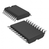
Renesas Electronics Corporation Gate Drivers R2J20652ANP#G3

Description
Gate Driver IC
Description
Gate Driver IC
Datasheet
Datasheet Summary
Powered by GS/AI

The R2J20652ANP#G3 is a multi-chip module that integrates a high-side MOS FET, low-side MOS FET, and a MOS-FET driver within a compact QFN package measuring 6 mm vó 6 mm vó 0.95 mm. This device is designed for high-current buck converter applications, making it suitable for use in notebooks, desktops, and servers. It features a built-in driver that optimizes the on and off timing of the power MOS FETs, enhancing performance. Key specifications include a maximum VIN operating voltage of 27 V and the capability to handle a large average output current of up to 35 A. The device supports high-frequency operation above 1 MHz and incorporates a low-side MOS FET with a built-in Schottky barrier diode (SBD) to minimize losses and reduce ringing. Additionally, it includes a tri-state input function compatible with various PWM controllers, a remote on/off control feature, and a low-side MOS FET disable function for discontinuous conduction mode (DCM) operation. The built-in bootstrap switch eliminates the need for an external SBD, further simplifying the design. The product is also Pb-free and halogen-free, aligning with environmental standards.

Datasheet Summary
Powered by GS/AI

The R2J20652ANP#G3 is a multi-chip module that integrates a high-side MOS FET, low-side MOS FET, and a MOS-FET driver within a compact QFN package measuring 6 mm vó 6 mm vó 0.95 mm. This device is designed for high-current buck converter applications, making it suitable for use in notebooks, desktops, and servers. It features a built-in driver that optimizes the on and off timing of the power MOS FETs, enhancing performance. Key specifications include a maximum VIN operating voltage of 27 V and the capability to handle a large average output current of up to 35 A. The device supports high-frequency operation above 1 MHz and incorporates a low-side MOS FET with a built-in Schottky barrier diode (SBD) to minimize losses and reduce ringing. Additionally, it includes a tri-state input function compatible with various PWM controllers, a remote on/off control feature, and a low-side MOS FET disable function for discontinuous conduction mode (DCM) operation. The built-in bootstrap switch eliminates the need for an external SBD, further simplifying the design. The product is also Pb-free and halogen-free, aligning with environmental standards.

Suppliers

Company
Product
Description
Supplier Links
Gate Drivers - R2J20652ANP#G3 - Quarktwin Technology Ltd.
Shenzhen, Guangdong, China
Gate Drivers
R2J20652ANP#G3
Gate Drivers R2J20652ANP#G3
Gate Driver IC

Gate Driver IC

Buy Now Datasheet

Technical Specifications

  Quarktwin Technology Ltd.
Product Category Gate Drivers
Product Number R2J20652ANP#G3
Product Name Gate Drivers
Output Configuration Inverting
Unlock Full Specs
to access all available technical data

Similar Products

Clock Buffers, Drivers - SI53354BD12750-AMR - Quarktwin Technology Ltd.
Specs
Output Configuration Inverting
Supply Voltage 1.71 to 3.46 volts
Switching Frequency 250000 kHz
View Details
Clock Buffers, Drivers - CDCLVP111MVFREP - Quarktwin Technology Ltd.
Specs
Output Configuration Inverting
Supply Voltage 2.38 to 3.8 volts
Switching Frequency 3.50E6 kHz
View Details
Gate Driver ICs - 1ED3131MC12H - Infineon Technologies AG
Infineon Technologies AG
Specs
Driver Type High-side
Output Current 5.5 amps
Supply Voltage 3.1 to 17 volts
View Details
 - 54ALS808AFK/B - Rochester Electronics
Rochester Electronics
Specs
Package Type LCC
Packing Method Tube; Tube; Other
View Details