pSemi Switch Evaluation Board EK4256-01

Description
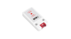
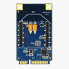
The SPDT Switch Evaluation Kit was designed to ease customer evaluation of the PE4256 SPDT switch. The RF common port (RFC) is connected through a 75 Ω transmission line to J2. Port 1 and Port 2 are connected through 75 Ω transmission lines to J1 and J3. A through transmission line connects F connectors J4 and J5. This transmission line can be used to estimate the loss of the PCB over the environmental conditions being evaluated. The board is constructed with four metal layers in FR4 material with a total thickness of 0.062”. The transmission lines were designed using a coplanar waveguide with ground plane (28 mil core, 21 mil width, 30 mil gap). J6 provides a means for controlling DC and digital inputs to the device. The provided jumpers short the package pin to ground for logic low. When the jumper is removed, the pin is pulled up to VDD for logic high. When the jumper is in place, 3 µA of current will flow through the 1 MΩ pull-up resistor. This extra current should not be attributed to the device. Proper PCB design is essential for full isolation performance. This evaluation board demonstrates good trace and ground management for minimum coupling and radiation.
Request a Quote Datasheet
Description
The SPDT Switch Evaluation Kit was designed to ease customer evaluation of the PE4256 SPDT switch. The RF common port (RFC) is connected through a 75 Ω transmission line to J2. Port 1 and Port 2 are connected through 75 Ω transmission lines to J1 and J3. A through transmission line connects F connectors J4 and J5. This transmission line can be used to estimate the loss of the PCB over the environmental conditions being evaluated. The board is constructed with four metal layers in FR4 material with a total thickness of 0.062”. The transmission lines were designed using a coplanar waveguide with ground plane (28 mil core, 21 mil width, 30 mil gap). J6 provides a means for controlling DC and digital inputs to the device. The provided jumpers short the package pin to ground for logic low. When the jumper is removed, the pin is pulled up to VDD for logic high. When the jumper is in place, 3 µA of current will flow through the 1 MΩ pull-up resistor. This extra current should not be attributed to the device. Proper PCB design is essential for full isolation performance. This evaluation board demonstrates good trace and ground management for minimum coupling and radiation.
Request a Quote Datasheet

Suppliers

Company
Product
Description
Supplier Links
Switch Evaluation Board - EK4256-01 - Richardson RFPD
Downers Grove, IL, United States
Switch Evaluation Board
EK4256-01
Switch Evaluation Board EK4256-01
The SPDT Switch Evaluation Kit was designed to ease customer evaluation of the PE4256 SPDT switch. The RF common port (RFC) is connected through a 75 Ω transmission line to J2. Port 1 and Port 2 are connected through 75 Ω transmission lines to J1 and J3. A through transmission line connects F connectors J4 and J5. This transmission line can be used to estimate the loss of the PCB over the environmental conditions being evaluated. The board is constructed with four metal layers in FR4 material with a total thickness of 0.062”. The transmission lines were designed using a coplanar waveguide with ground plane (28 mil core, 21 mil width, 30 mil gap). J6 provides a means for controlling DC and digital inputs to the device. The provided jumpers short the package pin to ground for logic low. When the jumper is removed, the pin is pulled up to VDD for logic high. When the jumper is in place, 3 µA of current will flow through the 1 MΩ pull-up resistor. This extra current should not be attributed to the device. Proper PCB design is essential for full isolation performance. This evaluation board demonstrates good trace and ground management for minimum coupling and radiation.

The SPDT Switch Evaluation Kit was designed to ease customer evaluation of the PE4256 SPDT switch. The RF common port (RFC) is connected through a 75 Ω transmission line to J2. Port 1 and Port 2 are connected through 75 Ω transmission lines to J1 and J3. A through transmission line connects F connectors J4 and J5. This transmission line can be used to estimate the loss of the PCB over the environmental conditions being evaluated. The board is constructed with four metal layers in FR4 material with a total thickness of 0.062”. The transmission lines were designed using a coplanar waveguide with ground plane (28 mil core, 21 mil width, 30 mil gap). J6 provides a means for controlling DC and digital inputs to the device. The provided jumpers short the package pin to ground for logic low. When the jumper is removed, the pin is pulled up to VDD for logic high. When the jumper is in place, 3 µA of current will flow through the 1 MΩ pull-up resistor. This extra current should not be attributed to the device. Proper PCB design is essential for full isolation performance. This evaluation board demonstrates good trace and ground management for minimum coupling and radiation.

Supplier's Site Datasheet

Technical Specifications

  Richardson RFPD
Product Category Electronic Development Boards
Product Number EK4256-01
Product Name Switch Evaluation Board
Category Developement Board
Unlock Full Specs
to access all available technical data

Similar Products

Development Tool Accessories - 2305134 - RS Components, Ltd.
Specs
Category Development Suite / Kit
View Details
HYT Evaluation Box - HYT Evaluation Box - Innovative Sensor Technology IST USA Division
Innovative Sensor Technology IST USA Division
Specs
Category Developement Board
View Details
Evaluation Boards - CY3679 - Infineon Technologies AG
Infineon Technologies AG
Specs
Category Developement Board
Supported System Industrial automation ; Communication ; Infotainment
View Details
3 suppliers