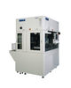
The XE-WAFER is a fully automated industrial AFM designed specifically to address surface roughness, trench width, depth, and angle measurements on 200mm & 300mm wafers in a production environment. The system provides superior accuracy and precision nanometrology over any other system in the market today. Providing the highest resolution and the lowest gauge sigma value for repeatability and reproducibility, the XE-WAFER is the perfect solution for the semiconductor and hard disk drive industries which, until now, had very limited choices for industrial grade in-line inspection tools.
Artifact Free Metrology by Crosstalk Elimination
• Two independent, closed-loop XY and Z flexure scanners for sample and tip
• Flat and linear XY scan of 100 μm x 100 μm with low residual bow
• Out of plane motion of less than 2 nm over entire scan range
• Accurate feature measurements with industry leading gauge sigma
• Superior tool to tool matching
Longer Tip Life by True Non-Contact Mode
• 10 times larger Z-scan bandwidth than a piezotube
• Less tip wear for prolonged high-quality and high-resolution imaging
• Minimized sample damage or modification
• Soft photoresist structures can be imaged non-destructively
• Immunity from parameter-dependent results observed in tapping imaging
Precision Critical Angle Measurements
• Precision calibration of Z-scan orthogonality
• Provides the angle measurement accuracy of less than 0.1 degrees
• Fully automatic Critical Angle Measurement acquisition and analysis software
High Throughput Inline Automation
• Allowable sample size: 200/300mm wafers
• Automatic data acquisition and analysis of critical angles, roughness and trench measurements
• Automatic tip exchange (optional)
• Equipment Front End Module (EFEM) for automatic wafer handling (optional)
• Cleanroom compatibility and remote control interface
| Park Systems, Inc. | |
|---|---|
| Product Category | Wafer and Thin Film Instrumentation |
| Product Name | XE-WAFER |
| Form Factor | Monitor or instrument |
| Mounting / Loading | Floor |
| Technology | Profilometer or AFM |