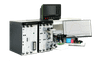
Hitachi High-Tech America Microspot XRF Ultra Thin Coating Analyzer FT160

Description
Microspot XRF coating thickness and materials analyzers for rapid quality control and validation testing, making it easy to get the right results in seconds. Coating thickness and materials analysis based on X-ray fluorescence (XRF) is a widely accepted and industry-proven analytical technique, offering easy-to-use, fast and non-destructive analysis, requiring little to no sample preparation, capable of analyzing solids or liquids over a wide element range from 13Al to 92U on the periodic table. FT160 High Resolution SDD Element range : Al - U Chamber design : closed XY stage options : motorized, wafer Largest sample : 600 x 600 x 20 mm Filters : 5 Polycarpellary optic spot size < 30 µm XRF Controller software
Datasheet
Description
Microspot XRF coating thickness and materials analyzers for rapid quality control and validation testing, making it easy to get the right results in seconds. Coating thickness and materials analysis based on X-ray fluorescence (XRF) is a widely accepted and industry-proven analytical technique, offering easy-to-use, fast and non-destructive analysis, requiring little to no sample preparation, capable of analyzing solids or liquids over a wide element range from 13Al to 92U on the periodic table. FT160 High Resolution SDD Element range : Al - U Chamber design : closed XY stage options : motorized, wafer Largest sample : 600 x 600 x 20 mm Filters : 5 Polycarpellary optic spot size < 30 µm XRF Controller software
Datasheet

Suppliers

Company
Product
Description
Supplier Links
Microspot XRF Ultra Thin Coating Analyzer - FT160 - Hitachi High-Tech America
Westford, MA, United States
Microspot XRF Ultra Thin Coating Analyzer
FT160
Microspot XRF Ultra Thin Coating Analyzer FT160
Microspot XRF coating thickness and materials analyzers for rapid quality control and validation testing, making it easy to get the right results in seconds. Coating thickness and materials analysis based on X-ray fluorescence (XRF) is a widely accepted and industry-proven analytical technique, offering easy-to-use, fast and non-destructive analysis, requiring little to no sample preparation, capable of analyzing solids or liquids over a wide element range from 13Al to 92U on the periodic table. FT160 High Resolution SDD Element range : Al - U Chamber design : closed XY stage options : motorized, wafer Largest sample : 600 x 600 x 20 mm Filters : 5 Polycarpellary optic spot size < 30 µm XRF Controller software

Microspot XRF coating thickness and materials analyzers for rapid quality control and validation testing, making it easy to get the right results in seconds.

Coating thickness and materials analysis based on X-ray fluorescence (XRF) is a widely accepted and industry-proven analytical technique, offering easy-to-use, fast and non-destructive analysis, requiring little to no sample preparation, capable of analyzing solids or liquids over a wide element range from 13Al to 92U on the periodic table.

FT160

  • High Resolution SDD
  • Element range : Al - U
  • Chamber design : closed
  • XY stage options : motorized, wafer
  • Largest sample : 600 x 600 x 20 mm
  • Filters : 5
  • Polycarpellary optic spot size < 30 µm
  • XRF Controller software
Supplier's Site Datasheet

Technical Specifications

  Hitachi High-Tech America
Product Category Wafer and Thin Film Instrumentation
Product Number FT160
Product Name Microspot XRF Ultra Thin Coating Analyzer
Form Factor Monitor or instrument
Mounting / Loading Manual loading
Technology X-ray Diffractometer
Applications Wafer; Electroplate
Unlock Full Specs
to access all available technical data

Similar Products

Pulsar600 - pulsar600 - Cosmic Equipment SpA
Cosmic Equipment SpA
Specs
Form Factor Monitor or instrument
Applications Wafer
View Details
DART™ (Direct Analysis in Real Time) -  - JEOL USA, Inc.
Specs
Form Factor Monitor or instrument
Mounting / Loading Floor
View Details
Wafer Edge Grinders - CVP-3000 Series - Daitron Co., Ltd.
Specs
Form Factor Monitor or instrument
Mounting / Loading Floor
Applications Wafer
View Details
Automated Optical Inspection System - nSPEC™ - Nanotronics Imaging
Specs
Form Factor ProbingSystem
Mounting / Loading Manual loading
Technology Optical / Imaging
View Details