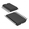
onsemi Clock Buffers, Drivers GTLP6C816MTC

Description
Clock Fanout Buffer (Distribution) IC 1:2, 1:6 24-TSSOP (0.173", 4.40mm Width)
Description
Clock Fanout Buffer (Distribution) IC 1:2, 1:6 24-TSSOP (0.173", 4.40mm Width)
Datasheet
Datasheet Summary
Powered by GS/AI

The GTLP6C816MTC is a clock driver designed for TTL to GTLP signal level translation and vice versa, facilitating high-speed communication between TTL logic level cards and GTLP logic level backplanes. It features a 1:2 clock driver path for TTL to GTLP translation and a 1:6 buffer for GTLP to TTL translation, with a single enable control for each direction. The device incorporates edge rate control circuitry to minimize output noise and ensure stable performance across variations in process, voltage, and temperature. The GTLP6C816MTC operates with a supply voltage of 5V and offers TTL-compatible driver and control inputs. It includes a V_REF pin for external reference voltage adjustment, and its outputs are designed to handle significant current, with the A port capable of sourcing and sinking up to 24mA and the B port sinking up to 50mA. The device is housed in a 24-lead Thin Shrink Small Outline Package (TSSOP), making it suitable for space-constrained applications. Engineers considering this product should note its compatibility with both TTL and GTLP logic levels, as well as its robust performance characteristics, which may be beneficial for high-speed digital applications.

Datasheet Summary
Powered by GS/AI

The GTLP6C816MTC is a clock driver designed for TTL to GTLP signal level translation and vice versa, facilitating high-speed communication between TTL logic level cards and GTLP logic level backplanes. It features a 1:2 clock driver path for TTL to GTLP translation and a 1:6 buffer for GTLP to TTL translation, with a single enable control for each direction. The device incorporates edge rate control circuitry to minimize output noise and ensure stable performance across variations in process, voltage, and temperature. The GTLP6C816MTC operates with a supply voltage of 5V and offers TTL-compatible driver and control inputs. It includes a V_REF pin for external reference voltage adjustment, and its outputs are designed to handle significant current, with the A port capable of sourcing and sinking up to 24mA and the B port sinking up to 50mA. The device is housed in a 24-lead Thin Shrink Small Outline Package (TSSOP), making it suitable for space-constrained applications. Engineers considering this product should note its compatibility with both TTL and GTLP logic levels, as well as its robust performance characteristics, which may be beneficial for high-speed digital applications.

Suppliers

Company
Product
Description
Supplier Links
Clock Buffers, Drivers - GTLP6C816MTC - Quarktwin Technology Ltd.
Shenzhen, Guangdong, China
Clock Buffers, Drivers
GTLP6C816MTC
Clock Buffers, Drivers GTLP6C816MTC
Clock Fanout Buffer (Distribution) IC 1:2, 1:6 24-TSSOP (0.173", 4.40mm Width)

Clock Fanout Buffer (Distribution) IC 1:2, 1:6 24-TSSOP (0.173", 4.40mm Width)

Buy Now Datasheet

Technical Specifications

  Quarktwin Technology Ltd.
Product Category Gate Drivers
Product Number GTLP6C816MTC
Product Name Clock Buffers, Drivers
Output Configuration Inverting
Unlock Full Specs
to access all available technical data

Similar Products

Gate Drivers - 1727-NGD4300DD-Q100JCT-ND - DigiKey
Specs
Driver Type Dual Gate Driver
Output Configuration Noninverting
Output Current 5 amps
View Details
Gate Drivers - 620-A89503KLPTR-5CT-ND - DigiKey
Allegro MicroSystems Inc.
Specs
Driver Type Dual Gate Driver
Output Configuration Noninverting
Supply Voltage 5.5 to 80 volts
View Details
5 suppliers
Gate Driver ICs - 6ED003L02-F2 - Infineon Technologies AG
Infineon Technologies AG
Specs
Driver Type Three-phase
Output Current 0.1650 amps
Supply Voltage 13 to 17.5 volts
View Details
4 suppliers