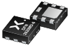

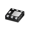
P-channel enhancement mode Field-Effect Transistor (FET) in a leadless medium power DFN2020MD-6 (SOT1220) Surface-Mounted Device (SMD) plastic package using Trench MOSFET technology, measuring 2 x 2 x 0.65 mm with an exposed drain pad for thermal conduction. The device is rated for a drain-source voltage of -20 V, a gate-source voltage range of -12 V to 12 V, and a continuous drain current of -5.5 A at 25 °C. It has a typical on-state resistance of 30 mΩ at -4.5 V gate drive and 25 °C, a total power dissipation of 1.7 W at 25 °C, and a junction temperature range of -55 °C to 150 °C. The package features tin-plated side pads for optical solder inspection and is suitable for applications including battery-powered portable devices, DC-to-DC converters, and power management in computing systems.
P-channel enhancement mode Field-Effect Transistor (FET) in a leadless medium power DFN2020MD-6 (SOT1220) Surface-Mounted Device (SMD) plastic package using Trench MOSFET technology.
Features and benefits
Applications
PMPB33XP/SOT1220/DFN
PMPB33XP/SOT1220/DFN
PMPB33XP/SOT1220/DFN
| Nexperia B.V. | DigiKey | |
|---|---|---|
| Product Category | Metal-Oxide Semiconductor FET (MOSFET) | Transistors |
| Product Number | PMPB33XPZ | 1727-PMPB33XPZTR-ND |
| Product Name | 20 V, single P-channel Trench MOSFET | Single FETs, MOSFETs |
| MOSFET Operating Mode | Enhancement | |
| V(BR)DSS | -20 volts | |
| IDSS | -7900 milliamps | |
| VGS(off) | 12 volts |
