Nexperia B.V. 12 V, P-channel Trench MOSFET PMPB14XPZ

Description
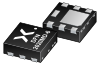
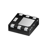
P-channel enhancement mode Field-Effect Transistor (FET) in a leadless medium power DFN2020MD-6 (SOT1220) Surface-Mounted Device (SMD) plastic package using Trench MOSFET technology. Features and benefits Low threshold voltage Trench MOSFET technology Side wettable flanks for optical solder inspection Small and leadless ultra thin SMD plastic package: 2 x 2 x 0.65 mm Exposed drain pad for excellent thermal conduction Applications Charging switch for portable devices DC-to-DC converters Power management in battery-driven portable devices Hard disk and computing power management
Request a Quote
Description
P-channel enhancement mode Field-Effect Transistor (FET) in a leadless medium power DFN2020MD-6 (SOT1220) Surface-Mounted Device (SMD) plastic package using Trench MOSFET technology. Features and benefits Low threshold voltage Trench MOSFET technology Side wettable flanks for optical solder inspection Small and leadless ultra thin SMD plastic package: 2 x 2 x 0.65 mm Exposed drain pad for excellent thermal conduction Applications Charging switch for portable devices DC-to-DC converters Power management in battery-driven portable devices Hard disk and computing power management
Request a Quote
Datasheet
Datasheet Summary
Powered by GS/AI

P-channel enhancement mode Field-Effect Transistor (FET) in a leadless medium power DFN2020MD-6 (SOT1220) Surface-Mounted Device (SMD) plastic package measuring 2 x 2 x 0.65 mm with an exposed drain pad for thermal conduction. It has a maximum drain-source voltage of -12 V, a gate-source voltage range of -8 to 8 V, and a continuous drain current of -8.6 A at 25 °C with V_GS = -4.5 V. The drain-source on-state resistance is 14 to 19 mΩ at V_GS = -4.5 V and I_D = -8.6 A. The device supports a peak drain current of -35 A in single pulses up to 10 µs and can dissipate up to 1.8 W continuously at 25 °C. It is rated for a junction temperature range of -55 to 150 °C and is suited for applications including portable device charging switches, DC-to-DC converters, and battery-powered power management.

Datasheet Summary
Powered by GS/AI

P-channel enhancement mode Field-Effect Transistor (FET) in a leadless medium power DFN2020MD-6 (SOT1220) Surface-Mounted Device (SMD) plastic package measuring 2 x 2 x 0.65 mm with an exposed drain pad for thermal conduction. It has a maximum drain-source voltage of -12 V, a gate-source voltage range of -8 to 8 V, and a continuous drain current of -8.6 A at 25 °C with V_GS = -4.5 V. The drain-source on-state resistance is 14 to 19 mΩ at V_GS = -4.5 V and I_D = -8.6 A. The device supports a peak drain current of -35 A in single pulses up to 10 µs and can dissipate up to 1.8 W continuously at 25 °C. It is rated for a junction temperature range of -55 to 150 °C and is suited for applications including portable device charging switches, DC-to-DC converters, and battery-powered power management.

Suppliers

Company
Product
Description
Supplier Links
12 V, P-channel Trench MOSFET - PMPB14XPZ - Nexperia B.V.
Nijmegen, Netherlands
12 V, P-channel Trench MOSFET
PMPB14XPZ
12 V, P-channel Trench MOSFET PMPB14XPZ
P-channel enhancement mode Field-Effect Transistor (FET) in a leadless medium power DFN2020MD-6 (SOT1220) Surface-Mounted Device (SMD) plastic package using Trench MOSFET technology. Features and benefits Low threshold voltage Trench MOSFET technology Side wettable flanks for optical solder inspection Small and leadless ultra thin SMD plastic package: 2 x 2 x 0.65 mm Exposed drain pad for excellent thermal conduction Applications Charging switch for portable devices DC-to-DC converters Power management in battery-driven portable devices Hard disk and computing power management

P-channel enhancement mode Field-Effect Transistor (FET) in a leadless medium power DFN2020MD-6 (SOT1220) Surface-Mounted Device (SMD) plastic package using Trench MOSFET technology.

Features and benefits

  • Low threshold voltage
  • Trench MOSFET technology
  • Side wettable flanks for optical solder inspection
  • Small and leadless ultra thin SMD plastic package: 2 x 2 x 0.65 mm
  • Exposed drain pad for excellent thermal conduction

Applications

  • Charging switch for portable devices
  • DC-to-DC converters
  • Power management in battery-driven portable devices
  • Hard disk and computing power management
Supplier's Site Datasheet
Single FETs, MOSFETs - 1727-PMPB14XPZTR-ND - DigiKey
Thief River Falls, MN, United States
Single FETs, MOSFETs
1727-PMPB14XPZTR-ND
Single FETs, MOSFETs 1727-PMPB14XPZTR-ND
PMPB14XP/SOT1220/SOT 1220

PMPB14XP/SOT1220/SOT1220

Buy Now Datasheet
Single FETs, MOSFETs - 1727-PMPB14XPZCT-ND - DigiKey
Thief River Falls, MN, United States
Single FETs, MOSFETs
1727-PMPB14XPZCT-ND
Single FETs, MOSFETs 1727-PMPB14XPZCT-ND
PMPB14XP/SOT1220/SOT 1220

PMPB14XP/SOT1220/SOT1220

Buy Now Datasheet
Single FETs, MOSFETs - 1727-PMPB14XPZDKR-ND - DigiKey
Thief River Falls, MN, United States
Single FETs, MOSFETs
1727-PMPB14XPZDKR-ND
Single FETs, MOSFETs 1727-PMPB14XPZDKR-ND
PMPB14XP/SOT1220/SOT 1220

PMPB14XP/SOT1220/SOT1220

Buy Now Datasheet

Technical Specifications

  Nexperia B.V. DigiKey
Product Category Metal-Oxide Semiconductor FET (MOSFET) Transistors
Product Number PMPB14XPZ 1727-PMPB14XPZTR-ND
Product Name 12 V, P-channel Trench MOSFET Single FETs, MOSFETs
MOSFET Operating Mode Enhancement
V(BR)DSS -12 volts
IDSS -12700 milliamps
VGS(off) 8 volts
Unlock Full Specs
to access all available technical data