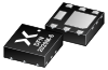
Nexperia B.V. 30 V, N-channel Trench MOSFET PMPB06R2ENZ

Description
N-channel enhancement mode Field-Effect Transistor (FET) in a leadless medium power DFN2020M-6 (SOT1220-2) Surface-Mounted Device (SMD) plastic package using Trench MOSFET technology. Features and benefits Logic-level compatible Ultra low QG, QGD for high system efficiency, especially at higher switching frequencies Superfast switching with soft-recovery Low spiking and ringing for low EMI designs Exposed drain pad for excellent thermal conduction Small and leadless ultra thin SMD plastic package: 2 x 2 x 0.65 mm Applications Intended for use in standard applications DC to DC conversion Battery management Low-side load switch Switching circuits
Request a Quote
Datasheet
Datasheet Summary
Powered by GS/AI

N-channel enhancement mode Field-Effect Transistor (FET) in a leadless medium power DFN2020M-6 (SOT1220-2) Surface-Mounted Device (SMD) plastic package measuring 2 x 2 x 0.65 mm, using Trench MOSFET technology. It has a drain-source voltage rating of 30 V, a continuous drain current of 18 A at 25 °C, and a drain-source on-state resistance of 6.2 to 7.4 mΩ at 10 V gate-source voltage and 25 °C. The device features an exposed drain pad for thermal conduction, logic-level compatibility, ultra-low gate charge for high switching efficiency, and superfast switching with soft-recovery. It meets the IEC 60134 Absolute Maximum Rating System and is intended for DC-to-DC conversion, battery management, low-side load switching, and general switching circuits.

Suppliers

Company
Product
Description
Supplier Links
30 V, N-channel Trench MOSFET - PMPB06R2ENZ - Nexperia B.V.
Nijmegen, Netherlands
30 V, N-channel Trench MOSFET
PMPB06R2ENZ
30 V, N-channel Trench MOSFET PMPB06R2ENZ
N-channel enhancement mode Field-Effect Transistor (FET) in a leadless medium power DFN2020M-6 (SOT1220-2) Surface-Mounted Device (SMD) plastic package using Trench MOSFET technology. Features and benefits Logic-level compatible Ultra low QG, QGD for high system efficiency, especially at higher switching frequencies Superfast switching with soft-recovery Low spiking and ringing for low EMI designs Exposed drain pad for excellent thermal conduction Small and leadless ultra thin SMD plastic package: 2 x 2 x 0.65 mm Applications Intended for use in standard applications DC to DC conversion Battery management Low-side load switch Switching circuits

N-channel enhancement mode Field-Effect Transistor (FET) in a leadless medium power DFN2020M-6 (SOT1220-2) Surface-Mounted Device (SMD) plastic package using Trench MOSFET technology.

Features and benefits

  • Logic-level compatible
  • Ultra low QG, QGD for high system efficiency, especially at higher switching frequencies
  • Superfast switching with soft-recovery
  • Low spiking and ringing for low EMI designs
  • Exposed drain pad for excellent thermal conduction
  • Small and leadless ultra thin SMD plastic package: 2 x 2 x 0.65 mm

Applications

  • Intended for use in standard applications
  • DC to DC conversion
  • Battery management
  • Low-side load switch
  • Switching circuits
Supplier's Site Datasheet
Single FETs, MOSFETs - 1727-PMPB06R2ENZTR-ND - DigiKey
Thief River Falls, MN, United States
Single FETs, MOSFETs
1727-PMPB06R2ENZTR-ND
Single FETs, MOSFETs 1727-PMPB06R2ENZTR-ND
PMPB06R2EN/SOT1220-2 /DFN2020M-

PMPB06R2EN/SOT1220-2/DFN2020M-

Buy Now Datasheet
Single FETs, MOSFETs - 1727-PMPB06R2ENZCT-ND - DigiKey
Thief River Falls, MN, United States
Single FETs, MOSFETs
1727-PMPB06R2ENZCT-ND
Single FETs, MOSFETs 1727-PMPB06R2ENZCT-ND
PMPB06R2EN/SOT1220-2 /DFN2020M-

PMPB06R2EN/SOT1220-2/DFN2020M-

Buy Now Datasheet
Single FETs, MOSFETs - 1727-PMPB06R2ENZDKR-ND - DigiKey
Thief River Falls, MN, United States
Single FETs, MOSFETs
1727-PMPB06R2ENZDKR-ND
Single FETs, MOSFETs 1727-PMPB06R2ENZDKR-ND
PMPB06R2EN/SOT1220-2 /DFN2020M-

PMPB06R2EN/SOT1220-2/DFN2020M-

Buy Now Datasheet

Technical Specifications

  Nexperia B.V. DigiKey
Product Category Metal-Oxide Semiconductor FET (MOSFET) Transistors
Product Number PMPB06R2ENZ 1727-PMPB06R2ENZTR-ND
Product Name 30 V, N-channel Trench MOSFET Single FETs, MOSFETs
MOSFET Operating Mode Enhancement
V(BR)DSS 30 volts
IDSS 18000 milliamps
VGS(off) 20 volts
Unlock Full Specs
to access all available technical data