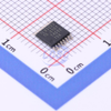
Nexperia B.V. Dual 1-of-4 multiplexer/demultiplexer 74CBTLV3253PW,118

Description
The 74CBTLV3253 provides a dual 1-of-4 high-speed multiplexer/demultip lexer with two common select inputs (S0, S1) and two output enable inputs (1OE, 2OE). The low ON resistance of the switch allows inputs to be connected to outputs without adding propagation delay or generating additional ground bounce noise. When pin nOE = LOW, one of the four switches is selected (low-impedance ON-state) with pins S0 and S1. When pin nOE = HIGH, all switches are in the high-impedance OFF-state, independent of pins S0 and S1. To ensure the high-impedance OFF-state during power-up or power-down, nOE should be tied to the VCC through a pull-up resistor. The minimum value of the resistor is determined by the current-sinking capability of the driver. Schmitt trigger action at control input makes the circuit tolerant to slower input rise and fall times across the entire VCC range from 2.3 V to 3.6 V. This device is fully specified for partial power-down applications using IOFF. The IOFF circuitry disables the output, preventing the damaging backflow current through the device when it is powered down. Features and benefits Supply voltage range from 2.3 V to 3.6 V High noise immunity Complies with JEDEC standard: JESD8-5 (2.3 V to 2.7 V) JESD8-B/JESD36 (2.7 V to 3.6 V) 5 Ω switch connection between two ports Rail to rail switching on data I/O ports CMOS low power consumption Latch-up performance exceeds 250 mA per JESD78B Class I level A IOFF circuitry provides partial Power-down mode operation ESD protection: HBM: ANSI/ESDA/JEDEC JS-001 class 2 exceeds 2000 V CDM: ANSI/ESDA/JEDEC JS-002 class C3 exceeds 1000 V Multiple package options Specified from -40 °C to +85 °C and -40 °C to +125 °C
Request a Quote Datasheet
Description
The 74CBTLV3253 provides a dual 1-of-4 high-speed multiplexer/demultip lexer with two common select inputs (S0, S1) and two output enable inputs (1OE, 2OE). The low ON resistance of the switch allows inputs to be connected to outputs without adding propagation delay or generating additional ground bounce noise. When pin nOE = LOW, one of the four switches is selected (low-impedance ON-state) with pins S0 and S1. When pin nOE = HIGH, all switches are in the high-impedance OFF-state, independent of pins S0 and S1. To ensure the high-impedance OFF-state during power-up or power-down, nOE should be tied to the VCC through a pull-up resistor. The minimum value of the resistor is determined by the current-sinking capability of the driver. Schmitt trigger action at control input makes the circuit tolerant to slower input rise and fall times across the entire VCC range from 2.3 V to 3.6 V. This device is fully specified for partial power-down applications using IOFF. The IOFF circuitry disables the output, preventing the damaging backflow current through the device when it is powered down. Features and benefits Supply voltage range from 2.3 V to 3.6 V High noise immunity Complies with JEDEC standard: JESD8-5 (2.3 V to 2.7 V) JESD8-B/JESD36 (2.7 V to 3.6 V) 5 Ω switch connection between two ports Rail to rail switching on data I/O ports CMOS low power consumption Latch-up performance exceeds 250 mA per JESD78B Class I level A IOFF circuitry provides partial Power-down mode operation ESD protection: HBM: ANSI/ESDA/JEDEC JS-001 class 2 exceeds 2000 V CDM: ANSI/ESDA/JEDEC JS-002 class C3 exceeds 1000 V Multiple package options Specified from -40 °C to +85 °C and -40 °C to +125 °C
Request a Quote Datasheet

Suppliers

Company
Product
Description
Supplier Links
Dual 1-of-4 multiplexer/demultiplexer - 74CBTLV3253PW,118 - Nexperia B.V.
Nijmegen, Netherlands
Dual 1-of-4 multiplexer/demultiplexer
74CBTLV3253PW,118
Dual 1-of-4 multiplexer/demultiplexer 74CBTLV3253PW,118
The 74CBTLV3253 provides a dual 1-of-4 high-speed multiplexer/demultip lexer with two common select inputs (S0, S1) and two output enable inputs (1OE, 2OE). The low ON resistance of the switch allows inputs to be connected to outputs without adding propagation delay or generating additional ground bounce noise. When pin nOE = LOW, one of the four switches is selected (low-impedance ON-state) with pins S0 and S1. When pin nOE = HIGH, all switches are in the high-impedance OFF-state, independent of pins S0 and S1. To ensure the high-impedance OFF-state during power-up or power-down, nOE should be tied to the VCC through a pull-up resistor. The minimum value of the resistor is determined by the current-sinking capability of the driver. Schmitt trigger action at control input makes the circuit tolerant to slower input rise and fall times across the entire VCC range from 2.3 V to 3.6 V. This device is fully specified for partial power-down applications using IOFF. The IOFF circuitry disables the output, preventing the damaging backflow current through the device when it is powered down. Features and benefits Supply voltage range from 2.3 V to 3.6 V High noise immunity Complies with JEDEC standard: JESD8-5 (2.3 V to 2.7 V) JESD8-B/JESD36 (2.7 V to 3.6 V) 5 Ω switch connection between two ports Rail to rail switching on data I/O ports CMOS low power consumption Latch-up performance exceeds 250 mA per JESD78B Class I level A IOFF circuitry provides partial Power-down mode operation ESD protection: HBM: ANSI/ESDA/JEDEC JS-001 class 2 exceeds 2000 V CDM: ANSI/ESDA/JEDEC JS-002 class C3 exceeds 1000 V Multiple package options Specified from -40 °C to +85 °C and -40 °C to +125 °C

The 74CBTLV3253 provides a dual 1-of-4 high-speed multiplexer/demultiplexer with two common select inputs (S0, S1) and two output enable inputs (1OE, 2OE). The low ON resistance of the switch allows inputs to be connected to outputs without adding propagation delay or generating additional ground bounce noise. When pin nOE = LOW, one of the four switches is selected (low-impedance ON-state) with pins S0 and S1. When pin nOE = HIGH, all switches are in the high-impedance OFF-state, independent of pins S0 and S1.

To ensure the high-impedance OFF-state during power-up or power-down, nOE should be tied to the VCC through a pull-up resistor. The minimum value of the resistor is determined by the current-sinking capability of the driver.

Schmitt trigger action at control input makes the circuit tolerant to slower input rise and fall times across the entire VCC range from 2.3 V to 3.6 V.

This device is fully specified for partial power-down applications using IOFF. The IOFF circuitry disables the output, preventing the damaging backflow current through the device when it is powered down.

Features and benefits

  • Supply voltage range from 2.3 V to 3.6 V
  • High noise immunity
  • Complies with JEDEC standard:
    • JESD8-5 (2.3 V to 2.7 V)
    • JESD8-B/JESD36 (2.7 V to 3.6 V)
  • 5 Ω switch connection between two ports
  • Rail to rail switching on data I/O ports
  • CMOS low power consumption
  • Latch-up performance exceeds 250 mA per JESD78B Class I level A
  • IOFF circuitry provides partial Power-down mode operation
  • ESD protection:
    • HBM: ANSI/ESDA/JEDEC JS-001 class 2 exceeds 2000 V
    • CDM: ANSI/ESDA/JEDEC JS-002 class C3 exceeds 1000 V
  • Multiple package options
  • Specified from -40 °C to +85 °C and -40 °C to +125 °C
Supplier's Site Datasheet
Singapore
TSSOP Analog Switch and Multiplexer IC
743-74CBTLV3253PW,118
TSSOP Analog Switch and Multiplexer IC 743-74CBTLV3253PW,118
Multiplexer/Demultip lexer Bus Switch 1-Element CMOS 8-IN 16-Pin TSSOP T/R Product overview: 74CBTLV3253PW,118 from Nexperia is an Analog Switch and Multiplexer IC for embedded electronics, industrial equipment, maintenance repair, OEM production, and component sourcing. It is useful for engineers and buyers comparing datasheets, replacement parts, BOM lines, package options, lifecycle status, and procurement availability. Key searchable attributes include TSSOP. Search-friendly keywords include Analog Switch and Multiplexer IC, Encoders, Decoders, Multiplexers & Demultiplexers, electronic component, datasheet, replacement part, TSSOP. This listing supports clearer product discovery for industrial, commercial, repair, automation, power, sensing, and embedded system projects. Product number 743-74CBTLV3253PW,11 8 can be used for catalog matching and distributor lookup.

Multiplexer/Demultiplexer Bus Switch 1-Element CMOS 8-IN 16-Pin TSSOP T/R Product overview: 74CBTLV3253PW,118 from Nexperia is an Analog Switch and Multiplexer IC for embedded electronics, industrial equipment, maintenance repair, OEM production, and component sourcing. It is useful for engineers and buyers comparing datasheets, replacement parts, BOM lines, package options, lifecycle status, and procurement availability. Key searchable attributes include TSSOP. Search-friendly keywords include Analog Switch and Multiplexer IC, Encoders, Decoders, Multiplexers & Demultiplexers, electronic component, datasheet, replacement part, TSSOP. This listing supports clearer product discovery for industrial, commercial, repair, automation, power, sensing, and embedded system projects. Product number 743-74CBTLV3253PW,118 can be used for catalog matching and distributor lookup.

Supplier's Site Datasheet
Signal Switches, Multiplexers, Decoders - 1727-4407-1-ND - DigiKey
Thief River Falls, MN, United States
Signal Switches, Multiplexers, Decoders
1727-4407-1-ND
Signal Switches, Multiplexers, Decoders 1727-4407-1-ND
Multiplexer/Demultip lexer 2 x 4:1 16-TSSOP

Multiplexer/Demultiplexer 2 x 4:1 16-TSSOP

Buy Now Datasheet
Signal Switches, Multiplexers, Decoders - 1727-4407-2-ND - DigiKey
Thief River Falls, MN, United States
Signal Switches, Multiplexers, Decoders
1727-4407-2-ND
Signal Switches, Multiplexers, Decoders 1727-4407-2-ND
Multiplexer/Demultip lexer 2 x 4:1 16-TSSOP

Multiplexer/Demultiplexer 2 x 4:1 16-TSSOP

Buy Now Datasheet
Signal Switches, Multiplexers, Decoders - 1727-4407-6-ND - DigiKey
Thief River Falls, MN, United States
Signal Switches, Multiplexers, Decoders
1727-4407-6-ND
Signal Switches, Multiplexers, Decoders 1727-4407-6-ND
Multiplexer/Demultip lexer 2 x 4:1 16-TSSOP

Multiplexer/Demultiplexer 2 x 4:1 16-TSSOP

Buy Now Datasheet
Logic ICs >> Signal Switches / Encoders & Decoders / Multiplexers - 74CBTLV3253PW,118 - LCSC Electronics Technology (HK) Limited
Futian, Shenzhen, China
Logic ICs >> Signal Switches / Encoders & Decoders / Multiplexers
74CBTLV3253PW,118
Logic ICs >> Signal Switches / Encoders & Decoders / Multiplexers 74CBTLV3253PW,118
2.3V~3.6V TSSOP-16 Signal Switches / Encoders & Decoders / Multiplexers ROHS

2.3V~3.6V TSSOP-16 Signal Switches / Encoders & Decoders / Multiplexers ROHS

Supplier's Site Datasheet
Logic - Signal Switches, Multiplexers, Decoders - 74CBTLV3253PW,118 - Lingto Electronic Limited
Shenzhen, China
Logic - Signal Switches, Multiplexers, Decoders
74CBTLV3253PW,118
Logic - Signal Switches, Multiplexers, Decoders 74CBTLV3253PW,118
IC MUX/DEMUX 2 X 4:1 16TSSOP

IC MUX/DEMUX 2 X 4:1 16TSSOP

Supplier's Site Datasheet

Technical Specifications

  Nexperia B.V. ERSAELECTRONICS PTE. LTD. DigiKey LCSC Electronics Technology (HK) Limited Lingto Electronic Limited
Product Category IC Analog Multiplexers IC Analog Multiplexers IC Analog Multiplexers IC Analog Multiplexers IC Analog Multiplexers
Product Number 74CBTLV3253PW,118 743-74CBTLV3253PW,118 1727-4407-1-ND 74CBTLV3253PW,118 74CBTLV3253PW,118
Product Name Dual 1-of-4 multiplexer/demultiplexer TSSOP Analog Switch and Multiplexer IC Signal Switches, Multiplexers, Decoders Logic ICs >> Signal Switches / Encoders & Decoders / Multiplexers Logic - Signal Switches, Multiplexers, Decoders
Features On-Chip ESD Protection
Standards and Certifications RoHS RoHS
Supply Voltage (VS) 2.3 to 3.6 volts 2.3 to 3.6 volts
Ron 7 ohms
Unlock Full Specs
to access all available technical data

Similar Products

Signal Switches, Multiplexers, Decoders - 1727-74CBTLVD3245BQ-Q1XTR-ND - DigiKey
Specs
Operating Temperature -40 to 125 C (-40 to 257 F)
Package Type 20-VFQFN
Number of Pins 20
View Details
Signal Switches, Multiplexers, Decoders - 568-8849-2-ND - DigiKey
Specs
Operating Temperature -40 to 125 C (-40 to 257 F)
Package Type SSOP; "24-SSOP
View Details
2 suppliers