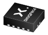
Nexperia B.V. Low-power Schmitt trigger 74AUP1G17GM,132

Description
The 74AUP1G17 is a single buffer with Schmitt-trigger input. This device ensures very low static and dynamic power consumption across the entire VCC range from 0.8 V to 3.6 V. This device is fully specified for partial power down applications using IOFF. The IOFF circuitry disables the output, preventing the potentially damaging backflow current through the device when it is powered down. Features and benefits Wide supply voltage range from 0.8 V to 3.6 V CMOS low power dissipation High noise immunity Overvoltage tolerant inputs to 3.6 V Low noise overshoot and undershoot < 10 % of VCC IOFF circuitry provides partial Power-down mode operation Latch-up performance exceeds 100 mA per JESD 78 Class II Level B Low static power consumption; ICC = 0.9 μA (maximum) Complies with JEDEC standards: JESD8-12 (0.8 V to 1.3 V) JESD8-11 (0.9 V to 1.65 V) JESD8-7 (1.2 V to 1.95 V) JESD8-5 (1.8 V to 2.7 V) JESD8C (2.7 V to 3.6 V) ESD protection: HBM: ANSI/ESDA/JEDEC JS-001 class 3A exceeds 5000 V CDM: ANSI/ESDA/JEDEC JS-002 class C3 exceeds 1000 V Multiple package options Specified from -40 ° C to +85 ° C and -40 ° C to +125 ° C
Request a Quote Datasheet
Description
The 74AUP1G17 is a single buffer with Schmitt-trigger input. This device ensures very low static and dynamic power consumption across the entire VCC range from 0.8 V to 3.6 V. This device is fully specified for partial power down applications using IOFF. The IOFF circuitry disables the output, preventing the potentially damaging backflow current through the device when it is powered down. Features and benefits Wide supply voltage range from 0.8 V to 3.6 V CMOS low power dissipation High noise immunity Overvoltage tolerant inputs to 3.6 V Low noise overshoot and undershoot < 10 % of VCC IOFF circuitry provides partial Power-down mode operation Latch-up performance exceeds 100 mA per JESD 78 Class II Level B Low static power consumption; ICC = 0.9 μA (maximum) Complies with JEDEC standards: JESD8-12 (0.8 V to 1.3 V) JESD8-11 (0.9 V to 1.65 V) JESD8-7 (1.2 V to 1.95 V) JESD8-5 (1.8 V to 2.7 V) JESD8C (2.7 V to 3.6 V) ESD protection: HBM: ANSI/ESDA/JEDEC JS-001 class 3A exceeds 5000 V CDM: ANSI/ESDA/JEDEC JS-002 class C3 exceeds 1000 V Multiple package options Specified from -40 ° C to +85 ° C and -40 ° C to +125 ° C
Request a Quote Datasheet

Suppliers

Company
Product
Description
Supplier Links
Low-power Schmitt trigger - 74AUP1G17GM,132 - Nexperia B.V.
Nijmegen, Netherlands
Low-power Schmitt trigger
74AUP1G17GM,132
Low-power Schmitt trigger 74AUP1G17GM,132
The 74AUP1G17 is a single buffer with Schmitt-trigger input. This device ensures very low static and dynamic power consumption across the entire VCC range from 0.8 V to 3.6 V. This device is fully specified for partial power down applications using IOFF. The IOFF circuitry disables the output, preventing the potentially damaging backflow current through the device when it is powered down. Features and benefits Wide supply voltage range from 0.8 V to 3.6 V CMOS low power dissipation High noise immunity Overvoltage tolerant inputs to 3.6 V Low noise overshoot and undershoot < 10 % of VCC IOFF circuitry provides partial Power-down mode operation Latch-up performance exceeds 100 mA per JESD 78 Class II Level B Low static power consumption; ICC = 0.9 μA (maximum) Complies with JEDEC standards: JESD8-12 (0.8 V to 1.3 V) JESD8-11 (0.9 V to 1.65 V) JESD8-7 (1.2 V to 1.95 V) JESD8-5 (1.8 V to 2.7 V) JESD8C (2.7 V to 3.6 V) ESD protection: HBM: ANSI/ESDA/JEDEC JS-001 class 3A exceeds 5000 V CDM: ANSI/ESDA/JEDEC JS-002 class C3 exceeds 1000 V Multiple package options Specified from -40 ° C to +85 ° C and -40 ° C to +125 ° C

The 74AUP1G17 is a single buffer with Schmitt-trigger input. This device ensures very low static and dynamic power consumption across the entire VCC range from 0.8 V to 3.6 V. This device is fully specified for partial power down applications using IOFF. The IOFF circuitry disables the output, preventing the potentially damaging backflow current through the device when it is powered down.

Features and benefits

  • Wide supply voltage range from 0.8 V to 3.6 V
  • CMOS low power dissipation
  • High noise immunity
  • Overvoltage tolerant inputs to 3.6 V
  • Low noise overshoot and undershoot < 10 % of VCC
  • IOFF circuitry provides partial Power-down mode operation
  • Latch-up performance exceeds 100 mA per JESD 78 Class II Level B
  • Low static power consumption; ICC = 0.9 μA (maximum)
  • Complies with JEDEC standards:
    • JESD8-12 (0.8 V to 1.3 V)
    • JESD8-11 (0.9 V to 1.65 V)
    • JESD8-7 (1.2 V to 1.95 V)
    • JESD8-5 (1.8 V to 2.7 V)
    • JESD8C (2.7 V to 3.6 V)
  • ESD protection:
    • HBM: ANSI/ESDA/JEDEC JS-001 class 3A exceeds 5000 V
    • CDM: ANSI/ESDA/JEDEC JS-002 class C3 exceeds 1000 V
  • Multiple package options
  • Specified from -40 ° C to +85 ° C and -40 ° C to +125 ° C
Supplier's Site Datasheet

Technical Specifications

  Nexperia B.V.
Product Category Logic Gates
Product Number 74AUP1G17GM,132
Product Name Low-power Schmitt trigger
Supply Voltage +4.6
Unlock Full Specs
to access all available technical data

Similar Products

Quad 2-input AND gate - 74AHC08BQ/GX - Nexperia B.V.
Specs
Gate Type AND
Supply Voltage +7.0
IC Package Type Other; SOT762-1 SOT762-1
View Details
Gates and Inverters - 1727-74AHC1G04GM,115TR-ND - DigiKey
Specs
Gate Type NOT
Supply Voltage 2V ~ 5.5V
Inputs 1
View Details
5 suppliers
8-bit Logic IC - 706-74AHCT374PW - ERSAELECTRONICS PTE. LTD.
Specs
Gate Type Buffer/Driver
Logic Family AHCT/VHCT
Operating Temperature -40 C (-40 F)
View Details