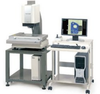
The Nanotronics Imaging nSpec® is an inspection device designed for high resolution microscopy and detection of wafer defects. With particular application in silicon carbide and Galium Nitride epi wafers, the nSpec® offers fast quantification and qualification of defects with detailed reporting and mapping. The system can be provided fully automated with multiple magnifications in order to fully characterize defect frequency and type. The system offers complete rapid scanning and mosaicing of wafers. Reports and statistical functions are easily defined by users and generated by nSpec®.
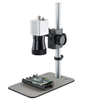
The hardware is critical in an inspection system. We use only the highest quality optics from the worlds’ leaders in microscopy including Nikon. We couple the optics with high resolution cameras for image capture and analysis. By high resolution we do not mean just a high number of megapixels, but high spatial resolution - the ability to discern small variances (link to the resolution nano-topic section of our site). With great optics and photo-microscopy we then add lighting to meet these demanding applications. Wavelengths can be chosen and light paths selected to optimize resolution and imaging requirements. Really, this is still all optics but we need to add some mechanics of focus and scanning. For this we manufacture our own precision translation stages and microscope stands.
The nSpec® can be used with Nanotronics' nPlace™ wafer transfer system, an automatic robot system. This system features interchangeable wafer chucks and a 25 piece loading capacity. Please see Nanotronics' web site for a video demonstration of the nPlace in action.
| Nanotronics Imaging | |
|---|---|
| Product Category | Imaging Workstations |
| Product Number | nSPEC™ |
| Product Name | Automated Optical Inspection System |
| System Type | Modular / PC-Based |
| Applications | Electronics or Semiconductor Inspection |
| Image Source | Optical Microscope |