Monocrystal, Inc. Sapphire Wafer

Description
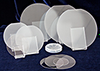
Due to its dielectric and crystallographic properties, sapphire is an outstanding material for producing various wafers for electronic applications. Sapphire is the basic material in LED production, as its crystal lattice allows the growth of an epitaxial layer of gallium nitride (GaN) with fine performance characteristics and a favorable price/quality ratio; also, it is considerably widely used. Among new and interesting applications of sapphire, it is worth mentioning the application of sapphire substrates in the production of blue semi-conductive lasers for systems requiring high-density data recording, for example, modern game consoles, Blue-ray players and other HD-DVD devices. Monocrystal provides 2", 3", 4", 6", 8" and 10" epi-polished wafers, as well as standard as cut/ground blanks made to customer specifications (miscut, with polished back surface, of different thickness). Wafers and blanks are produced from crystals grown using the Kyropoulos method. Advantages of our wafers: high material purity: > 99.997%; low impurity content Ti: < 1 ppm; low dislocation density: < 103 cm-2; orientation tolerance: up to ± 0.05 degrees. Sapphire wafers for semiconductive items are supplied with different orientations, including M, А, R, and C planes. Production of various shapes is possible (round, rectangular or square), from a few mm to 250 mm in diameter per customer specifications. Wafer thickness varies from 0.15 mm to 1.0 mm depending on the field of application. Our equipment enables the control of wafer production from the moment of crystal growth to manufacturing of the final product.
Description
Due to its dielectric and crystallographic properties, sapphire is an outstanding material for producing various wafers for electronic applications. Sapphire is the basic material in LED production, as its crystal lattice allows the growth of an epitaxial layer of gallium nitride (GaN) with fine performance characteristics and a favorable price/quality ratio; also, it is considerably widely used. Among new and interesting applications of sapphire, it is worth mentioning the application of sapphire substrates in the production of blue semi-conductive lasers for systems requiring high-density data recording, for example, modern game consoles, Blue-ray players and other HD-DVD devices. Monocrystal provides 2", 3", 4", 6", 8" and 10" epi-polished wafers, as well as standard as cut/ground blanks made to customer specifications (miscut, with polished back surface, of different thickness). Wafers and blanks are produced from crystals grown using the Kyropoulos method. Advantages of our wafers: high material purity: > 99.997%; low impurity content Ti: < 1 ppm; low dislocation density: < 103 cm-2; orientation tolerance: up to ± 0.05 degrees. Sapphire wafers for semiconductive items are supplied with different orientations, including M, А, R, and C planes. Production of various shapes is possible (round, rectangular or square), from a few mm to 250 mm in diameter per customer specifications. Wafer thickness varies from 0.15 mm to 1.0 mm depending on the field of application. Our equipment enables the control of wafer production from the moment of crystal growth to manufacturing of the final product.

Suppliers

Company
Product
Description
Supplier Links
Sapphire Wafer -  - Monocrystal, Inc.
Stavropol, Russia
Sapphire Wafer
Sapphire Wafer
Due to its dielectric and crystallographic properties, sapphire is an outstanding material for producing various wafers for electronic applications. Sapphire is the basic material in LED production, as its crystal lattice allows the growth of an epitaxial layer of gallium nitride (GaN) with fine performance characteristics and a favorable price/quality ratio; also, it is considerably widely used. Among new and interesting applications of sapphire, it is worth mentioning the application of sapphire substrates in the production of blue semi-conductive lasers for systems requiring high-density data recording, for example, modern game consoles, Blue-ray players and other HD-DVD devices. Monocrystal provides 2", 3", 4", 6", 8" and 10" epi-polished wafers, as well as standard as cut/ground blanks made to customer specifications (miscut, with polished back surface, of different thickness). Wafers and blanks are produced from crystals grown using the Kyropoulos method. Advantages of our wafers: high material purity: > 99.997%; low impurity content Ti: < 1 ppm; low dislocation density: < 103 cm-2; orientation tolerance: up to ± 0.05 degrees. Sapphire wafers for semiconductive items are supplied with different orientations, including M, А, R, and C planes. Production of various shapes is possible (round, rectangular or square), from a few mm to 250 mm in diameter per customer specifications. Wafer thickness varies from 0.15 mm to 1.0 mm depending on the field of application. Our equipment enables the control of wafer production from the moment of crystal growth to manufacturing of the final product.
Due to its dielectric and crystallographic properties, sapphire is an outstanding material for producing various wafers for electronic applications. Sapphire is the basic material in LED production, as its crystal lattice allows the growth of an epitaxial layer of gallium nitride (GaN) with fine performance characteristics and a favorable price/quality ratio; also, it is considerably widely used.

Among new and interesting applications of sapphire, it is worth mentioning the application of sapphire substrates in the production of blue semi-conductive lasers for systems requiring high-density data recording, for example, modern game consoles, Blue-ray players and other HD-DVD devices.

Monocrystal provides 2", 3", 4", 6", 8" and 10" epi-polished wafers, as well as standard as cut/ground blanks made to customer specifications (miscut, with polished back surface, of different thickness). Wafers and blanks are produced from crystals grown using the Kyropoulos method.

Advantages of our wafers:

  • high material purity: > 99.997%;
  • low impurity content Ti: < 1 ppm;
  • low dislocation density: < 103 cm-2;
  • orientation tolerance: up to ± 0.05 degrees.

Sapphire wafers for semiconductive items are supplied with different orientations, including M, А, R, and C planes. Production of various shapes is possible (round, rectangular or square), from a few mm to 250 mm in diameter per customer specifications.

Wafer thickness varies from 0.15 mm to 1.0 mm depending on the field of application. Our equipment enables the control of wafer production from the moment of crystal growth to manufacturing of the final product.

Supplier's Site

Technical Specifications

  Monocrystal, Inc.
Product Category Industrial Ceramic Materials
Product Name Sapphire Wafer
Material Type Sapphire
Unlock Full Specs
to access all available technical data

Similar Products

Piston/Sleeve Assemblies -  - Insaco, Inc.
Specs
Material Type Alumina; Sapphire
Shape / Form Custom Shape
View Details
Ceramic Beads - 5364062 - RS Components, Ltd.
RS Components, Ltd.
Specs
Material Type Ceramic
View Details
Alumina Bead, In-Vacuum, Accepts 0.045″ Dia Wire, Package = 1 Foot Length - A1429-1-C - MPF Products, INC.
Specs
Material Type Alumina
Applications HV / Electrical
View Details
Alumina wear resistant structural parts -  - Shenzhen Great Precision Ceramic CO., LTD.
Shenzhen Great Precision Ceramic CO., LTD.
Specs
Material Type Alumina
Applications HV / Electrical
View Details