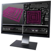
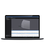
X.Tract provides CT-quality inspection results of complex, multilayer electronics assemblies without slicing the board. In a rapid and user friendly process, it creates virtual microsections in any direction in the region-of-interest. X.Tract reveals defects that are obscured in 2D X-ray images of layered components.
The new X.Tract tool provides, fully automated acquisition, powerful image processing and detailed reporting. With X.Tract, users gain better insight into complex packages such as Package on Package (PoP) or dual-layered boards leading to reduced false call rates and higher productivity.
Benefits
Identify defects with ease from complex multi-layer boards
Travel through a component by viewing 2D slices from any direction, enabling isolated clear views.
Works for small and large boards and assemblies
Automated, fast acquisition and view within minutes
Available on XT V 160 systems
Benefits & features
How X.Tract works
View in detail any virtual slice in any direction in an easy non-destructivePCBA, components or wafers are placed in an XT V X-ray inspection system and 2D images at submicron level are automatically taken 360° around the region-of-interest of the board. Image acquisition is complete within minutes and the 2D X-ray scans are reconstructed into a detailed 3D model.
This model can be sliced and analyzed in any plane using the X.Tract analysis tool. X.Tract technology provides high resolution, high magnifi cation CT functionality in the region-of-interest on the board – allowing users to accelerate product development, defect detection and inspection of complex packages.
Inspect further with X.Tract
X.Tract reveals defects that are obscured in 2D X-ray images of complex components such as Package on Package (PoP) or double sided boards. With X.Tract, users gain better insights leading to reduced false call rates and higher productivity.
Create virtual 3D micro sections of any region without slicing the board
Analyze multi-layer boards where 2D X-ray could obscure defect
Inspect complex packages such as BGA, PoP, CSP, QFN, LGA etc.
Isolate views for individual sides of a board which would normally show both board sides under 2D X-ray
Determine size and position of voids at joint interfaces or bulk solder
Easily identify hard-to-see defects such as Head-on-Pillow (HoP), open joints and cracks
Isolate views of the different layers within multi-layer packages such as Package on
Package (PoP) or multi-chip modules
Enable views of complex thru-hole components, connectors and board vias
Identify defects such as alignment and warpage
View individual board layers to analyze planes and tracks
X.Tract provides CT-quality inspection results of complex, multilayer electronics assemblies without slicing the board. In a rapid and user friendly process, it creates virtual microsections in any direction in the region-of-interest. X.Tract reveals defects that are obscured in 2D X-ray images of layered components.
The new X.Tract tool provides, fully automated acquisition, powerful image processing and detailed reporting. With X.Tract, users gain better insight into complex packages such as Package on Package (PoP) or dual-layered boards leading to reduced false call rates and higher productivity.
Benefits
- Identify defects with ease from complex multi-layer boards
- Travel through a component by viewing 2D slices from any direction, enabling isolated clear views.
- Works for small and large boards and assemblies
- Automated, fast acquisition and view within minutes
- Available on XT V 160 systems
Benefits & features
How X.Tract works
View in detail any virtual slice in any direction in an easy non-destructivePCBA, components or wafers are placed in an XT V X-ray inspection system and 2D images at submicron level are automatically taken 360° around the region-of-interest of the board. Image acquisition is complete within minutes and the 2D X-ray scans are reconstructed into a detailed 3D model.
This model can be sliced and analyzed in any plane using the X.Tract analysis tool. X.Tract technology provides high resolution, high magnifi cation CT functionality in the region-of-interest on the board – allowing users to accelerate product development, defect detection and inspection of complex packages.
Inspect further with X.Tract
X.Tract reveals defects that are obscured in 2D X-ray images of complex components such as Package on Package (PoP) or double sided boards. With X.Tract, users gain better insights leading to reduced false call rates and higher productivity.
- Create virtual 3D micro sections of any region without slicing the board
- Analyze multi-layer boards where 2D X-ray could obscure defect
- Inspect complex packages such as BGA, PoP, CSP, QFN, LGA etc.
- Isolate views for individual sides of a board which would normally show both board sides under 2D X-ray
- Determine size and position of voids at joint interfaces or bulk solder
- Easily identify hard-to-see defects such as Head-on-Pillow (HoP), open joints and cracks
- Isolate views of the different layers within multi-layer packages such as Package on
- Package (PoP) or multi-chip modules
- Enable views of complex thru-hole components, connectors and board vias
- Identify defects such as alignment and warpage
- View individual board layers to analyze planes and tracks