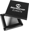
The ZL40272 is 3x12 HCSL/LVDS/LVPECL clock fan out buffer with ultra-low additive jitter of 24fs capable of operating at frequencies up to 1.5 GHz. Using the 12 output ZL40272 and utilizing the individual output pins or I2C interface, you can create hot-swappable PCIe clocktrees.
Applications include PCI Express generation 1/2/3/4/5 clock distribution, Intel QPI and UPI distribution, Servers, storage and data centers, switches and routers.
Additional Features
3 to 1 input Multiplexer: Two inputs accept any differential (LVPECL, HCSL, LVDS, SSTL, CML, LVCMOS) or a single ended signal and the third input accepts a crystal or a single ended signal
Twelve differential HCSL/LVDS/LVPECL outputs
Ultra-low additive jitter: 24fs (integration band: 12kHz to 20MHz at 625MHz clock frequency)
Supports clock frequencies from 0 to 1.5GHz
Supports 2.5V or 3.3V power supplies on HCSL/LVDS/LVPECL outputs
Embedded Low Drop Out (LDO) Voltage regulator provides superior Power Supply Noise Rejection
Maximum output to output skew of 50ps
Device controlled via I2C or hardware control pins
Factory configurable default settings via OTP
Transparent for spread spectrum clock
Applications
PCIe Gen1/2/3/4/5 clock distribution
Wired communications: OTN, SONET/SDH, GE, 10 GE, FC and 10G FC
General purpose clock distribution
Low jitter clock trees
Logic translation
Clock and data signal restoration
Wireless communications
High performance microprocessor clock distribution
Test Equipment
The ZL40272 is 3x12 HCSL/LVDS/LVPECL clock fan out buffer with ultra-low additive jitter of 24fs capable of operating at frequencies up to 1.5 GHz. Using the 12 output ZL40272 and utilizing the individual output pins or I2C interface, you can create hot-swappable PCIe clocktrees.
Applications include PCI Express generation 1/2/3/4/5 clock distribution, Intel QPI and UPI distribution, Servers, storage and data centers, switches and routers.
Additional Features
- 3 to 1 input Multiplexer: Two inputs accept any differential (LVPECL, HCSL, LVDS, SSTL, CML, LVCMOS) or a single ended signal and the third input accepts a crystal or a single ended signal
- Twelve differential HCSL/LVDS/LVPECL outputs
- Ultra-low additive jitter: 24fs (integration band: 12kHz to 20MHz at 625MHz clock frequency)
- Supports clock frequencies from 0 to 1.5GHz
- Supports 2.5V or 3.3V power supplies on HCSL/LVDS/LVPECL outputs
- Embedded Low Drop Out (LDO) Voltage regulator provides superior Power Supply Noise Rejection
- Maximum output to output skew of 50ps
- Device controlled via I2C or hardware control pins
- Factory configurable default settings via OTP
- Transparent for spread spectrum clock
- Applications
- PCIe Gen1/2/3/4/5 clock distribution
- Wired communications: OTN, SONET/SDH, GE, 10 GE, FC and 10G FC
- General purpose clock distribution
- Low jitter clock trees
- Logic translation
- Clock and data signal restoration
- Wireless communications
- High performance microprocessor clock distribution
- Test Equipment