Microchip Technology, Inc. Programmable 1:6 Multi-format Buffer ZL40251

Description
CREATE AND SAMPLE YOUR CUSTOM ZL40251 HERE ZL40251 6-output programmable fanout buffer with multi-format I/O and dividers offers the ability to create multiple copies of a clock signal and distribute them among several loads with minimal additive jitter. The ZL40251 features an intuitive graphical user interface (GUI) and the ability to create factory pre-programmed devices with ease using Microsemi’s web tool, miClockDesigner. These pre-programmed devices—which have pin-selectable configurations at power-up—ensure clock availability and proper system bring-up for all applications. Additional Features Four Flexible Input Clocks: one crystal/CMOS input, two differential/CMOS inputs, one single-ended/CMOS input Any input frequency up to 1GHz (300MHz for CMOS) Manual clock switching by pin or register 6 Universal Output Clocks with Dividers Each output has independent divider Low additive jitter <200fs RMS (12kHz-20MHz, for input frequencies above 100MHz) Each output configurable as LVDS, LVPECL, HCSL, 2xCMOS or HSTL In 2xCMOS mode, the P and N pins can be different frequencies (e.g. 125MHz and 25MHz) Multiple output supply voltage banks with CMOS output voltages from 1.5V to 3.3V Precise output alignment circuitry from GPIO pin or register bit Per-output skew adjustment Per-output enable/disable and glitchless start/stop (stop high or low) Automatic self-configuration at power-up from internal EEPROM; up to 8 configurations pin-selectable PCIe 1, 2, 3, 4 compliant Four multi-purpose I/O pins SPI or I2C processor Interface Core supply voltage options: 2.5V only, 3.3V only, 1.8V+2.5V or 1.8V+3.3V Space-saving 8x8mm QFN56 (0.5mm pitch) Easy-to-use evaluation/programmi ng software
Datasheet
Description
CREATE AND SAMPLE YOUR CUSTOM ZL40251 HERE ZL40251 6-output programmable fanout buffer with multi-format I/O and dividers offers the ability to create multiple copies of a clock signal and distribute them among several loads with minimal additive jitter. The ZL40251 features an intuitive graphical user interface (GUI) and the ability to create factory pre-programmed devices with ease using Microsemi’s web tool, miClockDesigner. These pre-programmed devices—which have pin-selectable configurations at power-up—ensure clock availability and proper system bring-up for all applications. Additional Features Four Flexible Input Clocks: one crystal/CMOS input, two differential/CMOS inputs, one single-ended/CMOS input Any input frequency up to 1GHz (300MHz for CMOS) Manual clock switching by pin or register 6 Universal Output Clocks with Dividers Each output has independent divider Low additive jitter <200fs RMS (12kHz-20MHz, for input frequencies above 100MHz) Each output configurable as LVDS, LVPECL, HCSL, 2xCMOS or HSTL In 2xCMOS mode, the P and N pins can be different frequencies (e.g. 125MHz and 25MHz) Multiple output supply voltage banks with CMOS output voltages from 1.5V to 3.3V Precise output alignment circuitry from GPIO pin or register bit Per-output skew adjustment Per-output enable/disable and glitchless start/stop (stop high or low) Automatic self-configuration at power-up from internal EEPROM; up to 8 configurations pin-selectable PCIe 1, 2, 3, 4 compliant Four multi-purpose I/O pins SPI or I2C processor Interface Core supply voltage options: 2.5V only, 3.3V only, 1.8V+2.5V or 1.8V+3.3V Space-saving 8x8mm QFN56 (0.5mm pitch) Easy-to-use evaluation/programmi ng software
Datasheet

Suppliers

Company
Product
Description
Supplier Links
Programmable 1:6 Multi-format Buffer - ZL40251 - Microchip Technology, Inc.
Chandler, AZ, United States
Programmable 1:6 Multi-format Buffer
ZL40251
Programmable 1:6 Multi-format Buffer ZL40251
CREATE AND SAMPLE YOUR CUSTOM ZL40251 HERE ZL40251 6-output programmable fanout buffer with multi-format I/O and dividers offers the ability to create multiple copies of a clock signal and distribute them among several loads with minimal additive jitter. The ZL40251 features an intuitive graphical user interface (GUI) and the ability to create factory pre-programmed devices with ease using Microsemi’s web tool, miClockDesigner. These pre-programmed devices—which have pin-selectable configurations at power-up—ensure clock availability and proper system bring-up for all applications. Additional Features Four Flexible Input Clocks: one crystal/CMOS input, two differential/CMOS inputs, one single-ended/CMOS input Any input frequency up to 1GHz (300MHz for CMOS) Manual clock switching by pin or register 6 Universal Output Clocks with Dividers Each output has independent divider Low additive jitter <200fs RMS (12kHz-20MHz, for input frequencies above 100MHz) Each output configurable as LVDS, LVPECL, HCSL, 2xCMOS or HSTL In 2xCMOS mode, the P and N pins can be different frequencies (e.g. 125MHz and 25MHz) Multiple output supply voltage banks with CMOS output voltages from 1.5V to 3.3V Precise output alignment circuitry from GPIO pin or register bit Per-output skew adjustment Per-output enable/disable and glitchless start/stop (stop high or low) Automatic self-configuration at power-up from internal EEPROM; up to 8 configurations pin-selectable PCIe 1, 2, 3, 4 compliant Four multi-purpose I/O pins SPI or I2C processor Interface Core supply voltage options: 2.5V only, 3.3V only, 1.8V+2.5V or 1.8V+3.3V Space-saving 8x8mm QFN56 (0.5mm pitch) Easy-to-use evaluation/programmi ng software

CREATE AND SAMPLE YOUR CUSTOM ZL40251 HERE

ZL40251 6-output programmable fanout buffer with multi-format I/O and dividers offers the ability to create multiple copies of a clock signal and distribute them among several loads with minimal additive jitter.
The ZL40251 features an intuitive graphical user interface (GUI) and the ability to create factory pre-programmed devices with ease using Microsemi’s web tool, miClockDesigner. These pre-programmed devices—which have pin-selectable configurations at power-up—ensure clock availability and proper system bring-up for all applications.

Additional Features

  • Four Flexible Input Clocks: one crystal/CMOS input, two differential/CMOS inputs, one single-ended/CMOS input
  • Any input frequency up to 1GHz (300MHz for CMOS)
  • Manual clock switching by pin or register
  • 6 Universal Output Clocks with Dividers
  • Each output has independent divider
  • Low additive jitter <200fs RMS (12kHz-20MHz, for input frequencies above 100MHz)
  • Each output configurable as LVDS, LVPECL, HCSL, 2xCMOS or HSTL
  • In 2xCMOS mode, the P and N pins can be different frequencies (e.g. 125MHz and 25MHz)
  • Multiple output supply voltage banks with CMOS output voltages from 1.5V to 3.3V
  • Precise output alignment circuitry from GPIO pin or register bit
  • Per-output skew adjustment
  • Per-output enable/disable and glitchless start/stop (stop high or low)
  • Automatic self-configuration at power-up from internal EEPROM; up to 8 configurations pin-selectable
  • PCIe 1, 2, 3, 4 compliant
  • Four multi-purpose I/O pins
  • SPI or I2C processor Interface
  • Core supply voltage options: 2.5V only, 3.3V only, 1.8V+2.5V or 1.8V+3.3V
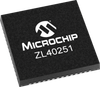
  • Space-saving 8x8mm QFN56 (0.5mm pitch)
  • Easy-to-use evaluation/programming software
Supplier's Site Datasheet

Technical Specifications

  Microchip Technology, Inc.
Product Category Amplifier and Comparator Chips
Product Number ZL40251
Product Name Programmable 1:6 Multi-format Buffer
Package Type ['VQFN']
Unlock Full Specs
to access all available technical data

Similar Products

Integrated Class D Audio Amplifier ICs - IR4301M - Infineon Technologies AG
Specs
Device Type Audio Amplifiers
Standards and Certifications RoHS
Package Type PQFN 22 pins
View Details
Log Amplifiers and DLVA - HCL-3-9001_2 - Crane Aerospace & Electronics
Crane Aerospace & Electronics
Specs
Device Type Log Amplifiers
View Details
Analog - MTLT1006AQD8 - Micross Components, Inc.
Micross Components, Inc.
Specs
Device Type Operational Amplifiers
View Details
20 GHz Rf Amplifier - 860-CMD201P5 - ERSAELECTRONICS PTE. LTD.
Specs
Device Type RF
Standards and Certifications RoHS
View Details