Microchip Technology, Inc. 1:2 LVDS Buffer ZL40212

Description
The ZL40212 is an LVDS clock fanout buffer with two identical output clock drivers capable of operating at frequencies up to 750MHz. Inputs to the ZL40212 are externally terminated to allow use of precision termination components and to allow full flexibility of input termination. The ZL40212 can accept DC coupled LVPECL or LVDS and AC coupled LVPECL, LVDS, CML or HCSL input signals; single ended input signals can also be accepted. A pin compatible device with internal termination is also available. The ZL40212 is designed to fan out low-jitter reference clocks for wired or optical communications applications while adding minimal jitter to the clock signal. An internal linear power supply regulator and bulk capacitors minimize additive jitter due to power supply noise. The device operates from 2.5V+/-5% or 3.3V+/-5% supply. Its operation is guaranteed over the industrial temperature range -40°C to +85°C. Additional Features Low additive jitter of 92 fs RMS Accepts differential or single-ended input: LVPECL, LVDS, CML, HCSL, LVCMOS Two precision LVDS outputs Operating frequency up to 750 MHz Options for 2.5 V or 3.3 V power supply wit6h current consumption of 44 mA On-chip Low Drop Out (LDO) Regulator for superior power supply noise rejection
Datasheet
Description
The ZL40212 is an LVDS clock fanout buffer with two identical output clock drivers capable of operating at frequencies up to 750MHz. Inputs to the ZL40212 are externally terminated to allow use of precision termination components and to allow full flexibility of input termination. The ZL40212 can accept DC coupled LVPECL or LVDS and AC coupled LVPECL, LVDS, CML or HCSL input signals; single ended input signals can also be accepted. A pin compatible device with internal termination is also available. The ZL40212 is designed to fan out low-jitter reference clocks for wired or optical communications applications while adding minimal jitter to the clock signal. An internal linear power supply regulator and bulk capacitors minimize additive jitter due to power supply noise. The device operates from 2.5V+/-5% or 3.3V+/-5% supply. Its operation is guaranteed over the industrial temperature range -40°C to +85°C. Additional Features Low additive jitter of 92 fs RMS Accepts differential or single-ended input: LVPECL, LVDS, CML, HCSL, LVCMOS Two precision LVDS outputs Operating frequency up to 750 MHz Options for 2.5 V or 3.3 V power supply wit6h current consumption of 44 mA On-chip Low Drop Out (LDO) Regulator for superior power supply noise rejection
Datasheet

Suppliers

Company
Product
Description
Supplier Links
1:2 LVDS Buffer - ZL40212 - Microchip Technology, Inc.
Chandler, AZ, United States
1:2 LVDS Buffer
ZL40212
1:2 LVDS Buffer ZL40212
The ZL40212 is an LVDS clock fanout buffer with two identical output clock drivers capable of operating at frequencies up to 750MHz. Inputs to the ZL40212 are externally terminated to allow use of precision termination components and to allow full flexibility of input termination. The ZL40212 can accept DC coupled LVPECL or LVDS and AC coupled LVPECL, LVDS, CML or HCSL input signals; single ended input signals can also be accepted. A pin compatible device with internal termination is also available. The ZL40212 is designed to fan out low-jitter reference clocks for wired or optical communications applications while adding minimal jitter to the clock signal. An internal linear power supply regulator and bulk capacitors minimize additive jitter due to power supply noise. The device operates from 2.5V+/-5% or 3.3V+/-5% supply. Its operation is guaranteed over the industrial temperature range -40°C to +85°C. Additional Features Low additive jitter of 92 fs RMS Accepts differential or single-ended input: LVPECL, LVDS, CML, HCSL, LVCMOS Two precision LVDS outputs Operating frequency up to 750 MHz Options for 2.5 V or 3.3 V power supply wit6h current consumption of 44 mA On-chip Low Drop Out (LDO) Regulator for superior power supply noise rejection
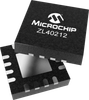
The ZL40212 is an LVDS clock fanout buffer with two identical output clock drivers capable of operating at frequencies up to 750MHz.

Inputs to the ZL40212 are externally terminated to allow use of precision termination components and to allow full flexibility of input termination. The ZL40212 can accept DC coupled LVPECL or LVDS and AC coupled LVPECL, LVDS, CML or HCSL input signals; single ended input signals can also be accepted. A pin compatible device with internal termination is also available.

The ZL40212 is designed to fan out low-jitter reference clocks for wired or optical communications applications while adding minimal jitter to the clock signal. An internal linear power supply regulator and bulk capacitors minimize additive jitter due to power supply noise. The device operates from 2.5V+/-5% or 3.3V+/-5% supply. Its operation is guaranteed over the industrial temperature range -40°C to +85°C.

Additional Features

  • Low additive jitter of 92 fs RMS
  • Accepts differential or single-ended input: LVPECL, LVDS, CML, HCSL, LVCMOS
  • Two precision LVDS outputs
  • Operating frequency up to 750 MHz
  • Options for 2.5 V or 3.3 V power supply wit6h current consumption of 44 mA
  • On-chip Low Drop Out (LDO) Regulator for superior power supply noise rejection

Supplier's Site Datasheet

Technical Specifications

  Microchip Technology, Inc.
Product Category Amplifier and Comparator Chips
Product Number ZL40212
Product Name 1:2 LVDS Buffer
Package Type ['VQFN']
Unlock Full Specs
to access all available technical data

Similar Products

5V 10V SOIC Linear Comparator IC - 692-LT1016CS8 - ERSAELECTRONICS PTE. LTD.
Specs
Device Type Comparators
Package Type Tube/Rail
View Details
Log Amplifiers and DLVA - HCL-4-9005_6 - Crane Aerospace & Electronics
Crane Aerospace & Electronics
Specs
Device Type Log Amplifiers
View Details
Analog - MTLT119AQH - Micross Components, Inc.
Micross Components, Inc.
Specs
Device Type Comparators
View Details