
The SY89847UMG is a precision LVDS fanout buffer designed to distribute clock signals with a 1:5 output configuration and features a 2:1 multiplexer. It operates at a supply voltage of 2.5V ¬±5% and is capable of handling input signals with a wide voltage range. The device supports a throughput of DC to over 1.5 GHz, with propagation delays guaranteed to be less than 1000 ps and rise/fall times under 210 ps. A notable feature is its fail-safe input, which prevents output oscillation when the input clock is invalid, ensuring reliable operation. The internal termination architecture allows for direct interfacing with various differential signals, including AC- and DC-coupled inputs, without the need for external termination resistors. The SY89847UMG is suitable for applications requiring ultra-low jitter clock distribution, with specifications indicating random jitter below 1 ps RMS and total jitter under 10 ps peak-to-peak. This component is housed in a compact 32-pin QFN package and is rated for an industrial temperature range of -40¬8C to +85¬8C, making it suitable for a variety of environments, including telecom and datacom applications.
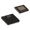
Clock Fanout Buffer (Distribution), Multiplexer IC 2:5 2 GHz 32-VFQFN Exposed Pad
| Quarktwin Technology Ltd. | |
|---|---|
| Product Category | Gate Drivers |
| Product Number | SY89847UMG |
| Product Name | Clock Buffers, Drivers |
| Output Configuration | Inverting |
| Supply Voltage | 2.38 to 2.62 volts |
| Switching Frequency | 2.00E6 kHz |