Microchip Technology, Inc. SY88063CL

Description
The SY88063CL limiting post amplifier is designed for use in fiber-optic receivers for multi-rate applications from 1.0625Gbps to 12.5Gbps. The SY88063CL contains a high-bandwidth, high-sensitivity input stage with user-programmable, wide-range SD assert/LOS de-assert threshold levels, which enables optimized system reach. Typically, 4dB of electrical hysteresis is provided to minimize LOS or SD chattering caused by noisy input signals. A logic level control pin is provided to enable user selection of an open-collector, TTL-compatible LOS or SD status indication signal with an external 5kΩ to 10kΩ pull-up resistor. The SY88063CL provides fast SD assert and LOS de-assert times over the entire differential input voltage range of 5mVPP to 1800mVPP. The SY88063CL input stage also provides a user-selectable digital offset correction (DOC) function to automatically compensate for internal device offsets in the high-speed data path. The SY88063CL provides integrated 50Ω input and output impedances to optimize the high-speed signal paths and reduce component count. A TTL-compatible JAM input is provided to enable a SQUELCH function by feeding back the LOS or SD signal. The JAM input disables only the post amplifier output. The SY88063CL operates from a single +3.3V power supply, over temperatures ranging from –40°C to +85°C. To request the datasheet, please email us at tcg_help@microchip.c om For product comparison, please consider: SY88083L Additional Features Multi-rate operation from 1.0625Gbps to 12.5Gbps Selectable digital offset correction for internal offset compensation in the high-speed data path Wide differential input range (5mVPP to 1800mVPP) Wide SD de-assert or LOS assert threshold range 3mVPP to 30mVPP 4dB typical electrical hysteresis Fast SD assert and LOS de-assert times 75ns typical; 120ns maximum Selectable LOS or SD status signal indicator TTL-compatible JAM input with internal pull-up Low-noise CML data inputs with integrated 50Ω termination impedance to internal reference VREF Low-noise CML data outputs with integrated 50Ω termination impedance 25ps typical rise/fall times Wide range power supply: 3.3V ±10% Industrial temperature range: -40°C to +85°C Available in a tiny 3mm x 3mm QFN package
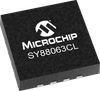
Description
The SY88063CL limiting post amplifier is designed for use in fiber-optic receivers for multi-rate applications from 1.0625Gbps to 12.5Gbps. The SY88063CL contains a high-bandwidth, high-sensitivity input stage with user-programmable, wide-range SD assert/LOS de-assert threshold levels, which enables optimized system reach. Typically, 4dB of electrical hysteresis is provided to minimize LOS or SD chattering caused by noisy input signals. A logic level control pin is provided to enable user selection of an open-collector, TTL-compatible LOS or SD status indication signal with an external 5kΩ to 10kΩ pull-up resistor. The SY88063CL provides fast SD assert and LOS de-assert times over the entire differential input voltage range of 5mVPP to 1800mVPP. The SY88063CL input stage also provides a user-selectable digital offset correction (DOC) function to automatically compensate for internal device offsets in the high-speed data path. The SY88063CL provides integrated 50Ω input and output impedances to optimize the high-speed signal paths and reduce component count. A TTL-compatible JAM input is provided to enable a SQUELCH function by feeding back the LOS or SD signal. The JAM input disables only the post amplifier output. The SY88063CL operates from a single +3.3V power supply, over temperatures ranging from –40°C to +85°C. To request the datasheet, please email us at tcg_help@microchip.c om For product comparison, please consider: SY88083L Additional Features Multi-rate operation from 1.0625Gbps to 12.5Gbps Selectable digital offset correction for internal offset compensation in the high-speed data path Wide differential input range (5mVPP to 1800mVPP) Wide SD de-assert or LOS assert threshold range 3mVPP to 30mVPP 4dB typical electrical hysteresis Fast SD assert and LOS de-assert times 75ns typical; 120ns maximum Selectable LOS or SD status signal indicator TTL-compatible JAM input with internal pull-up Low-noise CML data inputs with integrated 50Ω termination impedance to internal reference VREF Low-noise CML data outputs with integrated 50Ω termination impedance 25ps typical rise/fall times Wide range power supply: 3.3V ±10% Industrial temperature range: -40°C to +85°C Available in a tiny 3mm x 3mm QFN package

Suppliers

Company
Product
Description
Supplier Links
 - SY88063CL - Microchip Technology, Inc.
Chandler, AZ, United States
The SY88063CL limiting post amplifier is designed for use in fiber-optic receivers for multi-rate applications from 1.0625Gbps to 12.5Gbps. The SY88063CL contains a high-bandwidth, high-sensitivity input stage with user-programmable, wide-range SD assert/LOS de-assert threshold levels, which enables optimized system reach. Typically, 4dB of electrical hysteresis is provided to minimize LOS or SD chattering caused by noisy input signals. A logic level control pin is provided to enable user selection of an open-collector, TTL-compatible LOS or SD status indication signal with an external 5kΩ to 10kΩ pull-up resistor. The SY88063CL provides fast SD assert and LOS de-assert times over the entire differential input voltage range of 5mVPP to 1800mVPP. The SY88063CL input stage also provides a user-selectable digital offset correction (DOC) function to automatically compensate for internal device offsets in the high-speed data path. The SY88063CL provides integrated 50Ω input and output impedances to optimize the high-speed signal paths and reduce component count. A TTL-compatible JAM input is provided to enable a SQUELCH function by feeding back the LOS or SD signal. The JAM input disables only the post amplifier output. The SY88063CL operates from a single +3.3V power supply, over temperatures ranging from –40°C to +85°C. To request the datasheet, please email us at tcg_help@microchip.c om For product comparison, please consider: SY88083L Additional Features Multi-rate operation from 1.0625Gbps to 12.5Gbps Selectable digital offset correction for internal offset compensation in the high-speed data path Wide differential input range (5mVPP to 1800mVPP) Wide SD de-assert or LOS assert threshold range 3mVPP to 30mVPP 4dB typical electrical hysteresis Fast SD assert and LOS de-assert times 75ns typical; 120ns maximum Selectable LOS or SD status signal indicator TTL-compatible JAM input with internal pull-up Low-noise CML data inputs with integrated 50Ω termination impedance to internal reference VREF Low-noise CML data outputs with integrated 50Ω termination impedance 25ps typical rise/fall times Wide range power supply: 3.3V ±10% Industrial temperature range: -40°C to +85°C Available in a tiny 3mm x 3mm QFN package
The SY88063CL limiting post amplifier is designed for use in fiber-optic receivers for multi-rate applications from 1.0625Gbps to 12.5Gbps.

The SY88063CL contains a high-bandwidth, high-sensitivity input stage with user-programmable, wide-range SD assert/LOS de-assert threshold levels, which enables optimized system reach. Typically, 4dB of electrical hysteresis is provided to minimize LOS or SD chattering caused by noisy input signals. A logic level control pin is provided to enable user selection of an open-collector, TTL-compatible LOS or SD status indication signal with an external 5kΩ to 10kΩ pull-up resistor.

The SY88063CL provides fast SD assert and LOS de-assert times over the entire differential input voltage range of 5mVPP to 1800mVPP.

The SY88063CL input stage also provides a user-selectable digital offset correction (DOC) function to automatically compensate for internal device offsets in the high-speed data path.

The SY88063CL provides integrated 50Ω input and output impedances to optimize the high-speed signal paths and reduce component count. A TTL-compatible JAM input is provided to enable a SQUELCH function by feeding back the LOS or SD signal. The JAM input disables only the post amplifier output.

The SY88063CL operates from a single +3.3V power supply, over temperatures ranging from –40°C to +85°C.

To request the datasheet, please email us at tcg_help@microchip.com

For product comparison, please consider: SY88083L

Additional Features

  • Multi-rate operation from 1.0625Gbps to 12.5Gbps
  • Selectable digital offset correction for internal offset compensation in the high-speed data path
  • Wide differential input range (5mVPP to 1800mVPP)
  • Wide SD de-assert or LOS assert threshold range
    • 3mVPP to 30mVPP
    • 4dB typical electrical hysteresis
  • Fast SD assert and LOS de-assert times
    • 75ns typical; 120ns maximum
  • Selectable LOS or SD status signal indicator
  • TTL-compatible JAM input with internal pull-up
  • Low-noise CML data inputs with integrated 50Ω termination impedance to internal reference VREF
  • Low-noise CML data outputs with integrated 50Ω termination impedance
    • 25ps typical rise/fall times
  • Wide range power supply: 3.3V ±10%
  • Industrial temperature range: -40°C to +85°C
  • Available in a tiny 3mm x 3mm QFN package

Supplier's Site

Technical Specifications

  Microchip Technology, Inc.
Product Category Amplifier and Comparator Chips
Product Number SY88063CL
Package Type ['VQFN']
Unlock Full Specs
to access all available technical data

Similar Products

Dual Quad 50MHz 800V Operational Amplifier IC - 687-LT1362CN - ERSAELECTRONICS PTE. LTD.
Specs
Device Type Operational Amplifiers
View Details
Linear - Amplifiers - Instrumentation, OP Amps, Buffer Amps - 5962-9089401MEA - Lingto Electronic Limited
Specs
Device Type Instrumentation Amplifiers; Programmable Gain
View Details
Isolating amplifiers - 857-412 - WAGO
Specs
Device Type Isolaltion Amplifiers
View Details