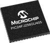
The PIC24FJ ‘GU4/GL4’ family offers up to 512KB of Dual Partition Flash supporting real-time Over-The-Air (OTA) updates and EEPROM Emulation. Along with a number of core independent peripherals (CIPs), it includes a full speed USB and a segmented LCD controller with animation support. With high memory and sleep current down to a few hundreds of nA while retaining the complete RAM content, this family is perfect for IoT, Industrial, Consumer and Medical applications. Supported in the MPLAB® Code Configurator (MCC) tool, the development time gets significantly reduced by allowing you to configure the devices and libraries with just a few clicks. To address the evolving focus on safety and security, these MCUs offer hardware safety features and secure protection schemes, simplifying design of smart, safe, secure and connected applications. These MCUs feature protection schemes such as Flash OTP by ICSP™ Write Inhibit which allows the entire Flash to be configured as One-Time-Programmabl
e (OTP) memory and CodeGuard™ Flash Security which facilitates to segment the memory and implement access restrictions. These features together with our CryptoAuthentication
™ chips enable you to implement security in your applications. Offering an extended operating temperature of up to 125°C with AEC Q100 Grade 1 qualification, this family is also well suited for Automotive and Industrial applications. A range of hardware safety features on this family facilitates your application’s compliance with safety requirements. With a high-level of analog integration, this family simplifies sensor interfacing and analog measurement, while reducing the overall system BoM cost.
Additional Features
Segmented LCD Controller with Animation
64 Segments and 8 Commons supporting up to 480 Pixels
Core independent autonomous animation: Alternating dual display, blinking and blanking
LCD Charge Pump for contrast management in battery-powered applications
External bias option for reducing power consumption
Operation in power-saving modes
Full Speed USB 2.0
Configurable as Host, Device or OTG
DMA Interface for Data RAM Access
Core and Operating Conditions
2.0V to 3.6V, -40°C to 125°C, AEC Q100 Grade 1 qualified, up to 16 MIPS operation
Single-cycle instruction execution
16 x 16 Hardware Multiply, and 32-bit x 16-bit Hardware Divider
C compiler optimized instruction set system
eXtreme Low Power
Ultra-low-power operation with sleep current down to nA with full RAM retention
A range of power-saving modes to reduce current consumption, while balancing performance: PMD bits, DOZE, Idle, Sleep and Retention Sleep modes
A range of Core Independent Peripherals (CIPs) that operate in power saving modes, while off-loading the Central Processing Unit (CPU)
Secure Protection Features
Flash ‘One Time Programming’ (OTP) by ICSP™ Write Inhibit that offers an ability to disable Flash erase/write/debug operations
CodeGuard™ Flash protection to manage memory partitions and access restrictions
120-bit Unique Device ID, 256 bytes User OTP and the above protection schemes make an ideal combination of complementary features to implement security together with the CryptoAuthentication
™ devices in a secure application
Hardware Safety Features
Flash with Error Correction Code (ECC) and Fault Injection for memory integrity check (Single error correction and Double error detection)
Dead-Man Timer (DMT) clocked by instruction fetches for monitoring the health of software
Windowed WatchDog Timer (WWDT) for system supervision
CodeGuard™ Flash protection for memory partition and access restriction
Fail-Safe Clock Monitor (FSCM) for clock fault management
Enhanced Programmable Cyclic Redundancy Check (CRC), Programmable High-Low Voltage Detect (HLVD), Brown-out Reset (BOR) and Power-on Reset (POR)
Class B Safety Library, IEC 60730
Advanced Integrated Analog
Up to 24-Channel, 400Ksps, 10/12-Bit Analog-to-Digital Converter (ADC)
Low-voltage boost for input
Bandgap reference input feature
Core Independent windowed threshold compare feature
Auto-scan feature
Operation in power-saving modes
Three Analog Comparators with input multiplexing and programmable reference voltage generators
Timer/Counters/Outpu
t Compare/Input Capture/Pulse Width Modulation
Eight MCCP modules, each with a Dedicated 16/32-Bit Timer
Three 6-output MCCP modules
Five 2-output MCCP modules
A total of up to 21x 16-bit timers or 10x 32-bit dedicated timer/counters
Hardware Real-Time Clock Calendar (RTCC) with Timestamping
Key Core Independent Peripherals
4x Configurable Logic Cells (CLCs)
8x Multiple Capture Compare PWMs (MCCPs)
Segmented LCD controller with Core Independent Animation, up to 480 pixels (8 commons x 64 segments)
ADC controller with threshold compare and automatic triggers
Direct Memory Access (DMA) with 6 channels, supporting UART, SPI, ADC, and more
Communication Interfaces
6x UARTs supporting LIN/J2602 and IrDA®
4x SPI/I2S, up to 24 MHz operation
3x I2C Master and Slave w/Address Masking, PMBus™ and IPMI support
Clock Management
On-chip 8 MHz Fast RC (FRC), and 32 kHz Low-Power RC (LPRC) and Secondary (SOSC) oscillators
Programmable PLL with external oscillator clock sources and Reference Clock Output (REFO)
Fail-Safe Clock Monitor (FSCM)
Power-up Timer (PWRT) and Oscillator Start-up Timer (OST) supporting two-speed start-up
Special Features and Debugger Development Support
MPLAB Code Configurator (MCC) support
Peripheral Pin Select (PPS) for flexible pin mapping
Configurable interrupt-on change on all IOs
In-Circuit Serial Programming™ (ICSP™) and In-Circuit Emulation (ICE) via 2-pins
JTAG Boundary Scan Support
The PIC24FJ ‘GU4/GL4’ family offers up to 512KB of Dual Partition Flash supporting real-time Over-The-Air (OTA) updates and EEPROM Emulation. Along with a number of core independent peripherals (CIPs), it includes a full speed USB and a segmented LCD controller with animation support. With high memory and sleep current down to a few hundreds of nA while retaining the complete RAM content, this family is perfect for IoT, Industrial, Consumer and Medical applications.
Supported in the MPLAB® Code Configurator (MCC) tool, the development time gets significantly reduced by allowing you to configure the devices and libraries with just a few clicks. To address the evolving focus on safety and security, these MCUs offer hardware safety features and secure protection schemes, simplifying design of smart, safe, secure and connected applications. These MCUs feature protection schemes such as Flash OTP by ICSP™ Write Inhibit which allows the entire Flash to be configured as One-Time-Programmable (OTP) memory and CodeGuard™ Flash Security which facilitates to segment the memory and implement access restrictions. These features together with our CryptoAuthentication™ chips enable you to implement security in your applications. Offering an extended operating temperature of up to 125°C with AEC Q100 Grade 1 qualification, this family is also well suited for Automotive and Industrial applications. A range of hardware safety features on this family facilitates your application’s compliance with safety requirements. With a high-level of analog integration, this family simplifies sensor interfacing and analog measurement, while reducing the overall system BoM cost.
Additional Features
- Segmented LCD Controller with Animation
- 64 Segments and 8 Commons supporting up to 480 Pixels
- Core independent autonomous animation: Alternating dual display, blinking and blanking
- LCD Charge Pump for contrast management in battery-powered applications
- External bias option for reducing power consumption
- Operation in power-saving modes
- Full Speed USB 2.0
- Configurable as Host, Device or OTG
- DMA Interface for Data RAM Access
- Core and Operating Conditions
- 2.0V to 3.6V, -40°C to 125°C, AEC Q100 Grade 1 qualified, up to 16 MIPS operation
- Single-cycle instruction execution
- 16 x 16 Hardware Multiply, and 32-bit x 16-bit Hardware Divider
- C compiler optimized instruction set system
- eXtreme Low Power
- Ultra-low-power operation with sleep current down to nA with full RAM retention
- A range of power-saving modes to reduce current consumption, while balancing performance: PMD bits, DOZE, Idle, Sleep and Retention Sleep modes
- A range of Core Independent Peripherals (CIPs) that operate in power saving modes, while off-loading the Central Processing Unit (CPU)
- Secure Protection Features
- Flash ‘One Time Programming’ (OTP) by ICSP™ Write Inhibit that offers an ability to disable Flash erase/write/debug operations
- CodeGuard™ Flash protection to manage memory partitions and access restrictions
- 120-bit Unique Device ID, 256 bytes User OTP and the above protection schemes make an ideal combination of complementary features to implement security together with the CryptoAuthentication™ devices in a secure application
- Hardware Safety Features
- Flash with Error Correction Code (ECC) and Fault Injection for memory integrity check (Single error correction and Double error detection)
- Dead-Man Timer (DMT) clocked by instruction fetches for monitoring the health of software
- Windowed WatchDog Timer (WWDT) for system supervision
- CodeGuard™ Flash protection for memory partition and access restriction
- Fail-Safe Clock Monitor (FSCM) for clock fault management
- Enhanced Programmable Cyclic Redundancy Check (CRC), Programmable High-Low Voltage Detect (HLVD), Brown-out Reset (BOR) and Power-on Reset (POR)
- Class B Safety Library, IEC 60730
- Advanced Integrated Analog
- Up to 24-Channel, 400Ksps, 10/12-Bit Analog-to-Digital Converter (ADC)
- Low-voltage boost for input
- Bandgap reference input feature
- Core Independent windowed threshold compare feature
- Auto-scan feature
- Operation in power-saving modes
- Three Analog Comparators with input multiplexing and programmable reference voltage generators
- Timer/Counters/Output Compare/Input Capture/Pulse Width Modulation
- Eight MCCP modules, each with a Dedicated 16/32-Bit Timer
- Three 6-output MCCP modules
- Five 2-output MCCP modules
- A total of up to 21x 16-bit timers or 10x 32-bit dedicated timer/counters
- Hardware Real-Time Clock Calendar (RTCC) with Timestamping
- Key Core Independent Peripherals
- 4x Configurable Logic Cells (CLCs)
- 8x Multiple Capture Compare PWMs (MCCPs)
- Segmented LCD controller with Core Independent Animation, up to 480 pixels (8 commons x 64 segments)
- ADC controller with threshold compare and automatic triggers
- Direct Memory Access (DMA) with 6 channels, supporting UART, SPI, ADC, and more
- Communication Interfaces
- 6x UARTs supporting LIN/J2602 and IrDA®
- 4x SPI/I2S, up to 24 MHz operation
- 3x I2C Master and Slave w/Address Masking, PMBus™ and IPMI support
- Clock Management
- On-chip 8 MHz Fast RC (FRC), and 32 kHz Low-Power RC (LPRC) and Secondary (SOSC) oscillators
- Programmable PLL with external oscillator clock sources and Reference Clock Output (REFO)
- Fail-Safe Clock Monitor (FSCM)
- Power-up Timer (PWRT) and Oscillator Start-up Timer (OST) supporting two-speed start-up
- Special Features and Debugger Development Support
- MPLAB Code Configurator (MCC) support
- Peripheral Pin Select (PPS) for flexible pin mapping
- Configurable interrupt-on change on all IOs
- In-Circuit Serial Programming™ (ICSP™) and In-Circuit Emulation (ICE) via 2-pins
- JTAG Boundary Scan Support