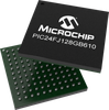
The eXtreme low power, PIC24F MCU includes up to 128KB of Flash memory with Error Correction Code (ECC) ,32 KB of RAM and USB connectivity. This device also features dual-partition Flash with Live Update capability, enabling them to hold two independent software applications, permitting simultaneous programming of one partition while executing application code from the other. With the ability to perform over-the-air firmware updates, designers can provide a cost-effective, reliable and secure method for updating their applications. These MCUs also feature eXtreme low power modes with current consumptions as low as 300nA in sleep modes. This powerful combination of features makes the PIC24F “GA6” family ideal for industrial, computer, medical/fitness and portable applications that require a long battery life, and data transfer and storage without the need of external memory, such as electricity metering, HVAC control, fingerprint scanners and gaming.
Additional Features
CPU
Modified Harvard Architecture
Up to 16 MIPS Operation @ 32 MHz
8 MHz Internal Oscillator:
96 MHz PLL option
Multiple clock divide options
Run-time self-calibration capability for maintaining better than ±0.20% accuracy
Fast start-up
17-Bit x 17-Bit Single-Cycle Hardware Fractional/Integer Multiplier
32-Bit by 16-Bit Hardware Divider
16 x 16-Bit Working Register Array
C Compiler Optimized Instruction Set Architecture
Two Address Generation Units for Separate Read and Write Addressing of Data Memory
Live Update
Dual Partition Flash with Live Update Capability
Capable of Holding Two Independent Software Applications, including Bootloader
Permits Simultaneous Programming of One Partition while Executing Application Code from the Other
Allows Run-Time Switching Between Active Partitions
Low-Power Features
Sleep and Idle modes Selectively Shut Down Peripherals and/or Core for Substantial Power Reduction and Fast Wake-up
Doze mode Allows CPU to Run at a Lower Clock Speed than Peripherals
Alternate Clock modes Allow On-the-Fly Switching to a Lower Clock Speed for Selective Power Reduction
Universal Serial Bus (USB) Features
USB v2.0 On-The-Go (OTG) Compliant
USB Device mode Operation from FRC Oscillator – No Crystal Oscillator Required
Low-Speed (1.5 Mb/s) and Full-Speed (12 Mb/s) USB Operation in Host mode
Supports up to 32 Endpoints (16 bidirectional)
Supports Control, Interrupt, Isochronous and Bulk Transfers
On-Chip Pull-up and Pull-Down Resistors
Analog Features
10/12-Bit, up to 24-Channel Analog-to-Digital (A/D) Converter:
12-bit conversion rate of 200 ksps
Auto-scan and threshold compare features
Conversion available during Sleep
Three Rail-to-Rail, Enhanced Analog Comparators with Programmable Input/Output Configuration
Charge Time Measurement Unit (CTMU):
Used for capacitive touch sensing, up to 24 channels
Time measurement down to 100 ps resolution
Peripheral Features
Peripheral Pin Select (PPS) –Allows Independent I/O Mapping of Many Peripherals
Eight-Channel DMA Supports All Peripheral modules
Six Input Capture modules, Each with a Dedicated 16-Bit Timer
Six Output Compare/PWM modules, Each with a Dedicated 16-Bit Timer
Four Single Output CCPs (SCCPs) and Three Multiple Output CCPs (MCCPs)
Enhanced Parallel Master/Slave Port (EPMP/EPSP)
Hardware Real-Time Clock/Calendar (RTCC) with Timestamping
Programmable 32-Bit Cyclic Redundancy Check (CRC) Generator
Four Configurable Logic Cells (CLCs)
5.5V Tolerant Inputs on Multiple I/O Pins
The eXtreme low power, PIC24F MCU includes up to 128KB of Flash memory with Error Correction Code (ECC) ,32 KB of RAM and USB connectivity. This device also features dual-partition Flash with Live Update capability, enabling them to hold two independent software applications, permitting simultaneous programming of one partition while executing application code from the other. With the ability to perform over-the-air firmware updates, designers can provide a cost-effective, reliable and secure method for updating their applications. These MCUs also feature eXtreme low power modes with current consumptions as low as 300nA in sleep modes.
This powerful combination of features makes the PIC24F “GA6” family ideal for industrial, computer, medical/fitness and portable applications that require a long battery life, and data transfer and storage without the need of external memory, such as electricity metering, HVAC control, fingerprint scanners and gaming.
Additional Features
- CPU
- Modified Harvard Architecture
- Up to 16 MIPS Operation @ 32 MHz
- 8 MHz Internal Oscillator:
- 96 MHz PLL option
- Multiple clock divide options
- Run-time self-calibration capability for maintaining better than ±0.20% accuracy
- Fast start-up
- 17-Bit x 17-Bit Single-Cycle Hardware Fractional/Integer Multiplier
- 32-Bit by 16-Bit Hardware Divider
- 16 x 16-Bit Working Register Array
- C Compiler Optimized Instruction Set Architecture
- Two Address Generation Units for Separate Read and Write Addressing of Data Memory
- Live Update
- Dual Partition Flash with Live Update Capability
- Capable of Holding Two Independent Software Applications, including Bootloader
- Permits Simultaneous Programming of One Partition while Executing Application Code from the Other
- Allows Run-Time Switching Between Active Partitions
- Low-Power Features
- Sleep and Idle modes Selectively Shut Down Peripherals and/or Core for Substantial Power Reduction and Fast Wake-up
- Doze mode Allows CPU to Run at a Lower Clock Speed than Peripherals
- Alternate Clock modes Allow On-the-Fly Switching to a Lower Clock Speed for Selective Power Reduction
- Universal Serial Bus (USB) Features
- USB v2.0 On-The-Go (OTG) Compliant
- USB Device mode Operation from FRC Oscillator – No Crystal Oscillator Required
- Low-Speed (1.5 Mb/s) and Full-Speed (12 Mb/s) USB Operation in Host mode
- Supports up to 32 Endpoints (16 bidirectional)
- Supports Control, Interrupt, Isochronous and Bulk Transfers
- On-Chip Pull-up and Pull-Down Resistors
- Analog Features
- 10/12-Bit, up to 24-Channel Analog-to-Digital (A/D) Converter:
- 12-bit conversion rate of 200 ksps
- Auto-scan and threshold compare features
- Conversion available during Sleep
- Three Rail-to-Rail, Enhanced Analog Comparators with Programmable Input/Output Configuration
- Charge Time Measurement Unit (CTMU):
- Used for capacitive touch sensing, up to 24 channels
- Time measurement down to 100 ps resolution
- Peripheral Features
- Peripheral Pin Select (PPS) –Allows Independent I/O Mapping of Many Peripherals
- Eight-Channel DMA Supports All Peripheral modules
- Six Input Capture modules, Each with a Dedicated 16-Bit Timer
- Six Output Compare/PWM modules, Each with a Dedicated 16-Bit Timer
- Four Single Output CCPs (SCCPs) and Three Multiple Output CCPs (MCCPs)
- Enhanced Parallel Master/Slave Port (EPMP/EPSP)
- Hardware Real-Time Clock/Calendar (RTCC) with Timestamping
- Programmable 32-Bit Cyclic Redundancy Check (CRC) Generator
- Four Configurable Logic Cells (CLCs)
- 5.5V Tolerant Inputs on Multiple I/O Pins