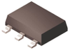
The MQ2N5114UB is a P-channel JFET in a low-profile ceramic surface mount package, designed for high-reliability applications with military screening per MIL-PRF-19500. It has a maximum drain-source voltage of 30 V and a steady-state power dissipation of 0.500 W at 25°C. The device features a gate-source breakdown voltage of 30 V and a drain current cutoff of -500 pA at 12 V gate-source bias. The package measures up to 0.128 inches in length and 0.108 inches in width, with a weight under 0.04 grams. Gold-plated terminals are standard, and the part is RoHS compliant when specified with the e3 suffix. Tape and reel packaging per EIA-418D is available. Switching characteristics include a turn-on delay time of 6 μs and a rise time of 10 μs.
| DigiKey | |
|---|---|
| Product Category | Transistors |
| Product Number | 150-MQ2N5114UB/TR-ND |
| Product Name | JFETs |
| Polarity | P-Channel |