The HV53001 device is an integrated driver solution for various applications, which consists of three main functional blocks (1) High voltage driver, (2) SPI interface and (3) DC/DC boost controller with power MOSFET.
The high voltage driver block includes 16 push-pull drivers capable of ±135V output swing with Return-To-Zero (RTZ) function. Each output driver is capable of sourcing and sinking at least 24mA. Each high voltage output is capable of driving up to 250 pF capacitive load. A global current sensor function is also integrated into this device to monitor the charge and discharge currents. The measured current is mapped to a low voltage analog output with a scale factor of 3.1 V/V via a current sensing resistor.
The SPI interface is used to communicate between the host processor and the high voltage drivers. This interface accepts a 3.3V logic I/O signal up to clock speed of 32MHz. Five digital LATCH control signals manage the data flow and the firing pattern. It establishes the output to one of four possible states: VPP, VNN, 0V or high impedance.
This IC also includes an integrated DC/DC controller with power MOSFET. The controller is used in a flyback configuration to generate four high voltage rails, ±135V and ±123V for the high voltage driver block. The ±123V rails are created from two 12V floating supplies referenced to the ±135V supply rails.
The converter accepts input voltage from a single 2.7V-5.5V input voltage rail. A built-in positive charge pump and a simple external negative charge pump convert the input supply to +6.5V and -6.0V supplies to power the high voltage driver block.
A proper power on and off sequence is critical to ensure the operation of the high voltage driver. A power sequence control circuit is included for the user to control the power supplies to power up or down the high voltage driver. It is used in conjunction with the external high voltage FET transistors.
Few safety features are added to the DC/DC converter. The over-voltage protection monitors both high voltage rails to protect the driver against over-voltage condition. A short circuit protection detects any short circuit event at the high voltage rails by monitoring the current flow through the power FET transistor. When a short circuit is detected, the DC/DC controller will shut down the converter and send a fault signal at the SHORT pin.
A over-temperature monitor function is also added in the converter IC. It sends a fault signal at the TEMP pin when it detects the temperature over the threshold temperature.
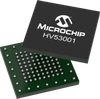
The HV53001 device is packaged in a 9x9mm 105 balls TFBGA package. All high voltage I/O are arranged to have sufficient clearance for safety.
Additional Features
16-Channel Push-Pull driver w/Return-To-Zero (RTZ) and High Impedance (Hi-Z) Function
Up to ±135V Output Voltage, w/24mA Minimum Source Sink Output Current (250 pF Cload Max)
Current Sensor Output
SPI Interface with Quad-Latch (2-Bit/Chanel) Architecture
Power-On Reset Function
Short Circuit Protection
Over-Temperature Monitor
Shutdown Function
105-ball 9 x 9 mm TFBGA Package
DC/DC Boost Converter with Power MOSFET (2.7V to 5.5Vin)
The HV53001 device is an integrated driver solution for various applications, which consists of three main functional blocks (1) High voltage driver, (2) SPI interface and (3) DC/DC boost controller with power MOSFET.
The high voltage driver block includes 16 push-pull drivers capable of ±135V output swing with Return-To-Zero (RTZ) function. Each output driver is capable of sourcing and sinking at least 24mA. Each high voltage output is capable of driving up to 250 pF capacitive load. A global current sensor function is also integrated into this device to monitor the charge and discharge currents. The measured current is mapped to a
low voltage analog output with a scale factor of 3.1 V/V via a current sensing resistor.
The SPI interface is used to communicate between the host processor and the high voltage drivers. This interface accepts a 3.3V logic I/O signal up to clock speed of 32MHz. Five digital LATCH control signals manage
the data flow and the firing pattern. It establishes the output to one of four possible states: VPP, VNN, 0V or high impedance.
This IC also includes an integrated DC/DC controller with power MOSFET. The controller is used in a flyback configuration to generate four high voltage rails, ±135V and ±123V for the high voltage driver block.
The ±123V rails are created from two 12V floating supplies referenced to the ±135V supply rails.
The converter accepts input voltage from a single 2.7V-5.5V input voltage rail. A built-in positive charge pump and a simple external negative charge pump convert the input supply to +6.5V and -6.0V supplies to power the high voltage driver block.
A proper power on and off sequence is critical to ensure the operation of the high voltage driver. A power sequence control circuit is included for the user to control the power supplies to power up or down the high
voltage driver. It is used in conjunction with the external high voltage FET transistors.
Few safety features are added to the DC/DC converter. The over-voltage protection monitors both high voltage rails to protect the driver against over-voltage condition. A short circuit protection detects any short circuit
event at the high voltage rails by monitoring the current flow through the power FET transistor. When a short circuit is detected, the DC/DC controller will shut down the converter and send a fault signal at the SHORT pin.
A over-temperature monitor function is also added in the converter IC. It sends a fault signal at the TEMP pin when it detects the temperature over the threshold temperature.
The HV53001 device is packaged in a 9x9mm 105 balls TFBGA package. All high voltage I/O are arranged to have sufficient clearance for safety.
Additional Features
- 16-Channel Push-Pull driver w/Return-To-Zero (RTZ) and High Impedance (Hi-Z) Function
- Up to ±135V Output Voltage, w/24mA Minimum Source Sink Output Current (250 pF Cload Max)
- Current Sensor Output
- SPI Interface with Quad-Latch (2-Bit/Chanel) Architecture
- Power-On Reset Function
- Short Circuit Protection
- Over-Temperature Monitor
- Shutdown Function
- 105-ball 9 x 9 mm TFBGA Package
- DC/DC Boost Converter with Power MOSFET (2.7V to 5.5Vin)