
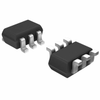
Littelfuse, Inc. Overvoltage Protection - TVS Diode Arrays - General Purpose - Series: SPUSB1 - SPUSB1BJT SPUSB1BJT

Description
The SPUSB1CJT and SPUSB1BJT are single-channel USB upstream-port termination networks. The SPUSB1 Series integrates EMI/RFI filter components R1 and C1, as recommended by the USB specification. Because these are upstream USB devices, they are terminated with a single 1.5K pull-resistor (R2) to VBUS. There are three options for the value of the series resistor R1: The SPUSB1AJT has R1=15?Ù¬ the SPUSB1CJT has R1=33?Ùand the SPUSB1BJT has R1=22?Ù® This series resistance must be close to the USB cable??s characteristic impedance of 45?Ù(90?Ùbalanced) to minimize transmission line reflections. In addition, these parts provide a very high level of protection for sensitive electronic components that may be subjected to electrostatic discharge (ESD). The input and output pins are designed and characterized to safely dissipate ESD strikes of 15kV, well beyond the maximum requirements of the IEC 61000-4-2 international standard. The VBUS pin is designed and characterized to safely dissipate ESD strikes of 25kV, according to the IEC 61000-4-2 international standard. The VBUS pin has greater ESD protection because in a USB connector, the VBUS prong is longer than the D+ and D- connector prongs and is first to make contact. Using the MIL-STD-883D (Method 3015) specification for Human Body Model (HBM) ESD, all pins are protected for contact discharges to greater than 30kV.
Request a Quote Datasheet
Description
The SPUSB1CJT and SPUSB1BJT are single-channel USB upstream-port termination networks. The SPUSB1 Series integrates EMI/RFI filter components R1 and C1, as recommended by the USB specification. Because these are upstream USB devices, they are terminated with a single 1.5K pull-resistor (R2) to VBUS. There are three options for the value of the series resistor R1: The SPUSB1AJT has R1=15?Ù¬ the SPUSB1CJT has R1=33?Ùand the SPUSB1BJT has R1=22?Ù® This series resistance must be close to the USB cable??s characteristic impedance of 45?Ù(90?Ùbalanced) to minimize transmission line reflections. In addition, these parts provide a very high level of protection for sensitive electronic components that may be subjected to electrostatic discharge (ESD). The input and output pins are designed and characterized to safely dissipate ESD strikes of 15kV, well beyond the maximum requirements of the IEC 61000-4-2 international standard. The VBUS pin is designed and characterized to safely dissipate ESD strikes of 25kV, according to the IEC 61000-4-2 international standard. The VBUS pin has greater ESD protection because in a USB connector, the VBUS prong is longer than the D+ and D- connector prongs and is first to make contact. Using the MIL-STD-883D (Method 3015) specification for Human Body Model (HBM) ESD, all pins are protected for contact discharges to greater than 30kV.
Request a Quote Datasheet

Suppliers

Company
Product
Description
Supplier Links
Overvoltage Protection - TVS Diode Arrays - General Purpose - Series: SPUSB1 - SPUSB1BJT - SPUSB1BJT - Littelfuse, Inc.
Rosemont, IL, United States
Overvoltage Protection - TVS Diode Arrays - General Purpose - Series: SPUSB1 - SPUSB1BJT
SPUSB1BJT
Overvoltage Protection - TVS Diode Arrays - General Purpose - Series: SPUSB1 - SPUSB1BJT SPUSB1BJT
The SPUSB1CJT and SPUSB1BJT are single-channel USB upstream-port termination networks. The SPUSB1 Series integrates EMI/RFI filter components R1 and C1, as recommended by the USB specification. Because these are upstream USB devices, they are terminated with a single 1.5K pull-resistor (R2) to VBUS. There are three options for the value of the series resistor R1: The SPUSB1AJT has R1=15?Ù¬ the SPUSB1CJT has R1=33?Ùand the SPUSB1BJT has R1=22?Ù® This series resistance must be close to the USB cable??s characteristic impedance of 45?Ù(90?Ùbalanced) to minimize transmission line reflections. In addition, these parts provide a very high level of protection for sensitive electronic components that may be subjected to electrostatic discharge (ESD). The input and output pins are designed and characterized to safely dissipate ESD strikes of 15kV, well beyond the maximum requirements of the IEC 61000-4-2 international standard. The VBUS pin is designed and characterized to safely dissipate ESD strikes of 25kV, according to the IEC 61000-4-2 international standard. The VBUS pin has greater ESD protection because in a USB connector, the VBUS prong is longer than the D+ and D- connector prongs and is first to make contact. Using the MIL-STD-883D (Method 3015) specification for Human Body Model (HBM) ESD, all pins are protected for contact discharges to greater than 30kV.

The SPUSB1CJT and SPUSB1BJT are single-channel USB upstream-port termination networks. The SPUSB1 Series integrates EMI/RFI filter components R1 and C1, as recommended by the USB specification. Because these are upstream USB devices, they are terminated with a single 1.5K pull-resistor (R2) to VBUS. There are three options for the value of the series resistor R1: The SPUSB1AJT has R1=15?Ù¬ the SPUSB1CJT has R1=33?Ùand the SPUSB1BJT has R1=22?Ù® This series resistance must be close to the USB cable??s characteristic impedance of 45?Ù(90?Ùbalanced) to minimize transmission line reflections. In addition, these parts provide a very high level of protection for sensitive electronic components that may be subjected to electrostatic discharge (ESD). The input and output pins are designed and characterized to safely dissipate ESD strikes of 15kV, well beyond the maximum requirements of the IEC 61000-4-2 international standard. The VBUS pin is designed and characterized to safely dissipate ESD strikes of 25kV, according to the IEC 61000-4-2 international standard. The VBUS pin has greater ESD protection because in a USB connector, the VBUS prong is longer than the D+ and D- connector prongs and is first to make contact. Using the MIL-STD-883D (Method 3015) specification for Human Body Model (HBM) ESD, all pins are protected for contact discharges to greater than 30kV.

Supplier's Site
Mixed Technology - SPUSB1BJT - ODG (Origin Data Global)
Shenzhen, China
Mixed Technology
SPUSB1BJT
Mixed Technology SPUSB1BJT
SURGE SUPPRESOR USB 22OHM SC70-6

SURGE SUPPRESOR USB 22OHM SC70-6

Supplier's Site Datasheet
Circuit Protection - Transient Voltage Suppressors (TVS) - Mixed Technology - SPUSB1BJT - Shenzhen Shengyu Electronics Technology Limited
Futian, China
Circuit Protection - Transient Voltage Suppressors (TVS) - Mixed Technology
SPUSB1BJT
Circuit Protection - Transient Voltage Suppressors (TVS) - Mixed Technology SPUSB1BJT
TVS DEVICE MIXED 8V SC70-6

TVS DEVICE MIXED 8V SC70-6

Supplier's Site

Technical Specifications

  Littelfuse, Inc. ODG (Origin Data Global) Shenzhen Shengyu Electronics Technology Limited
Product Category Diode Arrays Diodes Transient Voltage Suppressor Diodes (TVS)
Product Number SPUSB1BJT SPUSB1BJT SPUSB1BJT
Product Name Overvoltage Protection - TVS Diode Arrays - General Purpose - Series: SPUSB1 - SPUSB1BJT Mixed Technology Circuit Protection - Transient Voltage Suppressors (TVS) - Mixed Technology
Diode Type General Purpose; Transient Voltage Suppressor Diodes
Unlock Full Specs
to access all available technical data
