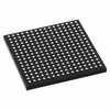


The LFXP2-5E-5FTN256C is a Field Programmable Gate Array (FPGA) from the LatticeXP2 family, featuring a flexiFLASH architecture that allows for instant-on capabilities and infinite reconfigurability. This device operates at a voltage of 1.2V and is packaged in a 256-ball ftBGA format. It includes 5,000 Look-Up Tables (LUTs) and supports a variety of I/O standards, including LVCMOS, LVTTL, SSTL, HSTL, PCI, and LVDS. The FPGA is equipped with embedded memory options, including up to 83 Kbits of distributed RAM and 885 Kbits of embedded block RAM (EBR). Additionally, it features sysDSP blocks for high-performance digital signal processing, with support for multiple 18x18 multipliers. The device also incorporates advanced security features such as 128-bit AES encryption and dual-boot capabilities, making it suitable for applications requiring secure updates. The LFXP2-5E-5FTN256C is designed for flexibility and efficiency, making it a viable option for engineers looking for a reliable FPGA solution.
FPGA 5000 Cells 311MHz 1.2V LBGA 172 I/O Product overview: LFXP2-5E-5FTN256C from Lattice Semiconductor is a FPGA Programmable Logic Device for real-time signal processing, programmable logic, communications, industrial automation, and custom hardware acceleration. It is useful for engineers and buyers comparing datasheets, replacement parts, BOM lines, package options, lifecycle status, and procurement availability. Key searchable attributes include 311MHz, 1.2V. Search-friendly keywords include FPGA, programmable logic, real-time signal processing, industrial automation, 311MHz, 1.2V, FPGA Programmable Logic Device, FPGAs. This listing supports clearer product discovery for industrial, commercial, repair, automation, power, sensing, and embedded system projects. Product number 696-LFXP2-5E-5FTN256
XP2 Field Programmable Gate Array (FPGA) IC 172 169984 5000 256-LBGA
Manufacturer: Lattice Semiconductor Corporation
Win Source Part Number: 070929-LFXP2-5E-5FTN
Mounting: SMD (SMT)
Number of I/O: 172
Number of LABs/CLBs: 625
Number of Logic Elements/Cells: 5000
Total RAM Bits: 169984
Family Name: LFXP2-5E
Categories: Integrated Circuits
Status: Active
Temperature Range - Operating: 0°C to 85°C (TJ)
Case / Package: 256-FTBGA (17x17)
Supply Voltage - Operating: 1.14 V to 1.26 V
Alternative Parts (Cross-Reference): A3P250L-1FG256; A3P250L-FGG256I; A3P600L-1FGG256YI ; A3P250L-1FG256I;
Introduction Date: May 20, 2009
ECCN: EAR99
Country of Origin: Malaysia
Estimated EOL Date: 2026
Halogen Free: Compliant
Is this a common-used part?: Yes
Popularity: High
Fake Threat In the Open Market: 60 pct.
Supply and Demand Status: Limited
IC FPGA 172 I/O 256FTBGA
IC FPGA 172 I/O 256FTBGA
XP2 Field Programmable Gate Array (FPGA) IC 172 169984 5000 256-LBGA
IC FPGA 172 I/O 256FTBGA
| ERSAELECTRONICS PTE. LTD. | DigiKey | Win Source Electronics | ODG (Origin Data Global) | Lingto Electronic Limited | Quarktwin Technology Ltd. | Shenzhen Shengyu Electronics Technology Limited | |
|---|---|---|---|---|---|---|---|
| Product Category | Field-Programmable Gate Arrays (FPGA) | Field-Programmable Gate Arrays (FPGA) | Field-Programmable Gate Arrays (FPGA) | Field-Programmable Gate Arrays (FPGA) | Field-Programmable Gate Arrays (FPGA) | Field-Programmable Gate Arrays (FPGA) | Field-Programmable Gate Arrays (FPGA) |
| Product Number | 696-LFXP2-5E-5FTN256C | 220-1247-ND | 070929-LFXP2-5E-5FTN256C | LFXP2-5E-5FTN256C | LFXP2-5E-5FTN256C | LFXP2-5E-5FTN256C | LFXP2-5E-5FTN256C |
| Product Name | 311MHz 1.2V FPGA Programmable Logic Device | FPGAs (Field Programmable Gate Array) | Embedded - Embedded - FPGAs (Field Programmable Gate Array) - LFXP2-5E-5FTN256C | FPGAs (Field Programmable Gate Array) | Embedded - FPGAs (Field Programmable Gate Array) | FPGAs (Field Programmable Gate Array) | Integrated Circuits (ICs) - Embedded - FPGAs (Field Programmable Gate Array) |
| Logic Cells / Logic Blocks | 5000 | 5000 | 5000 | 5000 | |||
| Package Type | Other; LBGA | Other; 256-LBGA | Other; 256-FTBGA (17x17) | Other; 256-LBGA | Other; 256-LBGA | ||
| Internal Frequency | 200 MHz | ||||||
| User I/Os | 172 pins | 172 pins | 172 pins | ||||
| Operating Temperature | 0 C (32 F) | 0 to 85 C (32 to 185 F) | 0 to 85 C (32 to 185 F) | 0 to 85 C (32 to 185 F) | 0 to 85 C (32 to 185 F) |