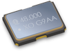
Integrated Device Technology Quad-Frequency Programmable VCXO 8N4QV01BG-0001CD

Description
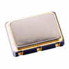
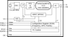
The 8N4QV01 is a Quad-Frequency Programmable VCXO with very flexible frequency and pull-range programming capabilities. The device uses IDT 's fourth generation FemtoClock® NG technology for an optimum of high clock frequency and low phase noise performance. The device accepts 2.5V or 3.3V supply and is packaged in a small, lead-free (RoHS 6) 10-lead ceramic 5mm x 7mm x 1.55mm package. Besides the 4 default power-up frequencies set by the FSEL0 and FSEL1 pins, the 8N4QV01 can be programmed via the I2C interface to any output clock frequency between 15.476MHz to 866.67MHz and from 975MHz to 1,300MHz to a very high degree of precision with a frequency step size of 435.9Hz ÷N (N is the PLL output divider). Since the FSEL0 and FSEL1 pins are mapped to 4 independent PLL , P, M and N divider registers (P, MINT , MFRAC and N), reprogramming those registers to other frequencies under control of FSEL0 and FSEL1 is supported. The extended temperature range supports wireless infrastructure, telecommunication and networking end equipment requirements.
Datasheet
Description
The 8N4QV01 is a Quad-Frequency Programmable VCXO with very flexible frequency and pull-range programming capabilities. The device uses IDT 's fourth generation FemtoClock® NG technology for an optimum of high clock frequency and low phase noise performance. The device accepts 2.5V or 3.3V supply and is packaged in a small, lead-free (RoHS 6) 10-lead ceramic 5mm x 7mm x 1.55mm package. Besides the 4 default power-up frequencies set by the FSEL0 and FSEL1 pins, the 8N4QV01 can be programmed via the I2C interface to any output clock frequency between 15.476MHz to 866.67MHz and from 975MHz to 1,300MHz to a very high degree of precision with a frequency step size of 435.9Hz ÷N (N is the PLL output divider). Since the FSEL0 and FSEL1 pins are mapped to 4 independent PLL , P, M and N divider registers (P, MINT , MFRAC and N), reprogramming those registers to other frequencies under control of FSEL0 and FSEL1 is supported. The extended temperature range supports wireless infrastructure, telecommunication and networking end equipment requirements.
Datasheet

Suppliers

Company
Product
Description
Supplier Links
Quad-Frequency Programmable VCXO - 8N4QV01BG-0001CD - Integrated Device Technology
San Jose, CA, USA
Quad-Frequency Programmable VCXO
8N4QV01BG-0001CD
Quad-Frequency Programmable VCXO 8N4QV01BG-0001CD
The 8N4QV01 is a Quad-Frequency Programmable VCXO with very flexible frequency and pull-range programming capabilities. The device uses IDT 's fourth generation FemtoClock® NG technology for an optimum of high clock frequency and low phase noise performance. The device accepts 2.5V or 3.3V supply and is packaged in a small, lead-free (RoHS 6) 10-lead ceramic 5mm x 7mm x 1.55mm package. Besides the 4 default power-up frequencies set by the FSEL0 and FSEL1 pins, the 8N4QV01 can be programmed via the I2C interface to any output clock frequency between 15.476MHz to 866.67MHz and from 975MHz to 1,300MHz to a very high degree of precision with a frequency step size of 435.9Hz ÷N (N is the PLL output divider). Since the FSEL0 and FSEL1 pins are mapped to 4 independent PLL , P, M and N divider registers (P, MINT , MFRAC and N), reprogramming those registers to other frequencies under control of FSEL0 and FSEL1 is supported. The extended temperature range supports wireless infrastructure, telecommunication and networking end equipment requirements.

The 8N4QV01 is a Quad-Frequency Programmable VCXO with very flexible frequency and pull-range programming capabilities. The device uses IDT 's fourth generation FemtoClock® NG technology for an optimum of high clock frequency and low phase noise performance. The device accepts 2.5V or 3.3V supply and is packaged in a small, lead-free (RoHS 6) 10-lead ceramic 5mm x 7mm x 1.55mm package. Besides the 4 default power-up frequencies set by the FSEL0 and FSEL1 pins, the 8N4QV01 can be programmed via the I2C interface to any output clock frequency between 15.476MHz to 866.67MHz and from 975MHz to 1,300MHz to a very high degree of precision with a frequency step size of 435.9Hz ÷N (N is the PLL output divider). Since the FSEL0 and FSEL1 pins are mapped to 4 independent PLL , P, M and N divider registers (P, MINT , MFRAC and N), reprogramming those registers to other frequencies under control of FSEL0 and FSEL1 is supported. The extended temperature range supports wireless infrastructure, telecommunication and networking end equipment requirements.

Supplier's Site Datasheet

Technical Specifications

  Integrated Device Technology
Product Category Oscillators
Product Number 8N4QV01BG-0001CD
Product Name Quad-Frequency Programmable VCXO
Oscillator Type VCXO
Package / Form Factor Surface Mount; CLCC
Features / Standards Lead-Free
Frequency 15.48 to 1300 MHz
Unlock Full Specs
to access all available technical data

Similar Products

VOLTAGE CONT OSC / RoHS - POS-150+ - Mini-Circuits
Specs
Features / Standards RoHS
Operating Temperature -55 to 85 C (-67 to 185 F)
View Details
kTB Low Phase Noise (PDRO) - PDRO50L - kTB Solutions
Specs
Oscillator Type DRO
Package / Form Factor Module
Frequency 1000 to 16000 MHz
View Details
Clock/Timing - Programmable Timers and Oscillators - LM555CMX/NOPB - Lingto Electronic Limited
Specs
Package / Form Factor Surface Mount; Surface Mount
Frequency 0.1000 MHz
Operating Temperature 0 to 70 C (32 to 158 F)
View Details
Clock/Timing - Programmable Timers and Oscillators - CY2X014LXI156T - Lingto Electronic Limited
Specs
Package / Form Factor Surface Mount; Surface Mount
Frequency 156 MHz
Operating Temperature -40 to 85 C (-40 to 185 F)
View Details
2 suppliers