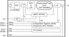

The 8N0QV01 is a Quad-Frequency Programmable VCXO with very flexible frequency and pull-range programming capabilities. The device uses IDT ’s Fourth Generation FemtoClock® NG technology for an optimum of high clock frequency and low phase noise performance. The device accepts 2.5V or 3.3V supply and ispackaged in a small, lead-free (RoHS 6) 10-lead ceramic 5mm x 7mm x 1.55mm package.
Besides the four default power-up frequencies set by the FSEL0 and FSEL1 pins, the 8N0QV01 can be programmed via the I2C interface to any output clock frequency between 15.476MHz to 260MHz to a very high degree of precision with a frequency step size of 435.9Hz ÷N (N: PLL post divider). Since the FSEL0 and FSEL1 pins are mapped to four independent PLL , P, M and N divider registers (P, MINT , MFRAC and N), reprogramming those registers to other frequencies under control of FSEL0 and FSEL1 is supported. The extended temperature range supports wireless infrastructure, telecommunication and networking end equipment requirements.
| Integrated Device Technology | |
|---|---|
| Product Category | Oscillators |
| Product Number | 8N0QV01KH-0098CDI |
| Product Name | Quad-Frequency Programmable VCXO |
| Oscillator Type | VCXO |
| Package / Form Factor | Surface Mount; CLCC |
| Features / Standards | Lead-Free |
| Frequency | 15.48 to 260 MHz |