Integrated Device Technology 512 x 18 SyncFIFO, 3.3V 72V215L15TFGI8

Description
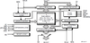
The 72V215 is a 512 x 18 first-in, first-out memory with clocked read and write controls. It is a 3.3V version of the 72215 FIFO and is applicable for a wide variety of data buffering needs, such as optical disk controllers, Local Area Networks (LANs), and interprocessor communication. It has 18-bit input and output ports. The Read Clock( RCLK ) can be tied to the Write Clock for single clock operation or the two clocks can run asynchronous of one another for dual-clock operation.
Datasheet
Description
The 72V215 is a 512 x 18 first-in, first-out memory with clocked read and write controls. It is a 3.3V version of the 72215 FIFO and is applicable for a wide variety of data buffering needs, such as optical disk controllers, Local Area Networks (LANs), and interprocessor communication. It has 18-bit input and output ports. The Read Clock( RCLK ) can be tied to the Write Clock for single clock operation or the two clocks can run asynchronous of one another for dual-clock operation.
Datasheet

Suppliers

Company
Product
Description
Supplier Links
512 x 18 SyncFIFO, 3.3V - 72V215L15TFGI8 - Integrated Device Technology
San Jose, CA, USA
512 x 18 SyncFIFO, 3.3V
72V215L15TFGI8
512 x 18 SyncFIFO, 3.3V 72V215L15TFGI8
The 72V215 is a 512 x 18 first-in, first-out memory with clocked read and write controls. It is a 3.3V version of the 72215 FIFO and is applicable for a wide variety of data buffering needs, such as optical disk controllers, Local Area Networks (LANs), and interprocessor communication. It has 18-bit input and output ports. The Read Clock( RCLK ) can be tied to the Write Clock for single clock operation or the two clocks can run asynchronous of one another for dual-clock operation.

The 72V215 is a 512 x 18 first-in, first-out memory with clocked read and write controls. It is a 3.3V version of the 72215 FIFO and is applicable for a wide variety of data buffering needs, such as optical disk controllers, Local Area Networks (LANs), and interprocessor communication. It has 18-bit input and output ports. The Read Clock( RCLK ) can be tied to the Write Clock for single clock operation or the two clocks can run asynchronous of one another for dual-clock operation.

Supplier's Site Datasheet

Technical Specifications

  Integrated Device Technology
Product Category Memory Chips
Product Number 72V215L15TFGI8
Product Name 512 x 18 SyncFIFO, 3.3V
Memory Category FIFO
Logic Family TTL
Data Rate 66 MHz
Operating Temperature -40 to 85 C (-40 to 185 F)
Density 9 kbits
Unlock Full Specs
to access all available technical data

Similar Products

SMV512K32-SP 16MB Radiation-Hardened SRAM - SMV512K32HFG/EM - Texas Instruments
Specs
Memory Category SRAM Chip
Access Time 20 ns
Density 16000 kbits
View Details
 - 4164-12JDS/BEA - Rochester Electronics
Rochester Electronics
Specs
Memory Category DRAM Chip
Package Type DIP; CDIP16
View Details
3 suppliers
Memory - 5962-9459901MYA - ODG (Origin Data Global)
Infineon Technologies AG
Specs
Memory Category NVSRAM (Non-Volatile SRAM); SRAM Chip
Access Time 55 ns
Operating Temperature -55 to 125 C (-67 to 257 F)
View Details
Memory - AS5SS256K18 - Micross Components, Inc.
Micross Components, Inc.
Specs
Memory Category SSRAM; SRAM Chip
Operating Temperature -55 to 125 C (-67 to 257 F)
Density 2048 kbits
View Details