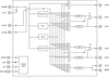
The 5V49EE702 is a programmable clock generator intended for high performance data-communications, telecommunications, consumer, and networking applications. There are four internal PLLs, each individually programmable, allowing for four unique non-integer-related frequencies. The frequencies are generated from a single reference clock. The reference clock can come from one of the two redundant clock inputs. Automatic or manual switchover function allows any one of the redundant clocks to be selected during normal operation. The 5V49EE702 is in-system, programmable and can be programmed through the use of I2C interface. An internal EEPROM allows the user to save and restore the configuration of the device without having to reprogram it on power-up. Each of the four PLLs has an 7-bit reference divider and a 12-bit feedback divider. This allows the user to generate four unique non-integer-related frequencies. The PLL loop bandwidth is programmable to allow the user to tailor the PLL response to the application. For instance, the user can tune the PLL parameters to minimize jitter generation or to maximize jitter attenuation. Spread spectrum generation and/or fractional divides are allowed on two of the PLLs. There are a total of five 8-bit output dividers. Each output bank can be configured to support LVTTL , LVPECL , LVDS or HCSL logic levels. Out0 (Output 0) supports LVTTL standard only. The outputs are connected to the PLLs via a switch matrix. The switch matrix allows the user to route the PLL outputs to any output bank. This feature can be used to simplify and optimize the board layout. In addition, each output's slew rate and enable/disable function is programmable.
The 5V49EE702 is a programmable clock generator intended for high performance data-communications, telecommunications, consumer, and networking applications. There are four internal PLLs, each individually programmable, allowing for four unique non-integer-related frequencies. The frequencies are generated from a single reference clock. The reference clock can come from one of the two redundant clock inputs. Automatic or manual switchover function allows any one of the redundant clocks to be selected during normal operation. The 5V49EE702 is in-system, programmable and can be programmed through the use of I2C interface. An internal EEPROM allows the user to save and restore the configuration of the device without having to reprogram it on power-up. Each of the four PLLs has an 7-bit reference divider and a 12-bit feedback divider. This allows the user to generate four unique non-integer-related frequencies. The PLL loop bandwidth is programmable to allow the user to tailor the PLL response to the application. For instance, the user can tune the PLL parameters to minimize jitter generation or to maximize jitter attenuation. Spread spectrum generation and/or fractional divides are allowed on two of the PLLs. There are a total of five 8-bit output dividers. Each output bank can be configured to support LVTTL , LVPECL , LVDS or HCSL logic levels. Out0 (Output 0) supports LVTTL standard only. The outputs are connected to the PLLs via a switch matrix. The switch matrix allows the user to route the PLL outputs to any output bank. This feature can be used to simplify and optimize the board layout. In addition, each output's slew rate and enable/disable function is programmable.