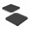
Infineon Technologies AG MOTIX™ MCU | 32-bit motor control SoC (system-on-chip) - H-Bridge Driver IC with integrated Arm® Cortex®-M - TLE9883-2QTW62S TLE9883-2QTW62S

Description
The MOTIX™ TLE9883-2QTW62S is designed to drive up to four external power NFETs The MOTIX™ TLE9883-2QTW62S is part of the MOTIX™ TLE988x product family. It is a fully integrated 2-Phase motor driver with the industry standard Arm® Cortex®-M3 core, enabling the implementation of advanced motor control algorithms. It includes a bridge-driver to drive up to four external power NFETs for 2-Phase motor control. A dual stage charge pump enables low voltage operation and programmable charge current profile along with adaptive MOSFET control for optimized EMC. Its peripheral set includes a current sense amplifier, two successive approximation ADCs that can be synchronized with the capture and compare unit 7 for PWM generation and several 16-bit timers. A CAN-FD transceiver and MULTICAN+ controller are integrated as well to enable CAN-FD communication along with a number of general purpose I/Os. It includes an on-chip linear voltage regulator to supply external loads. The safe switch of path developed according to ASIL-B enables to safely turn off the motor. It is a highly integrated AEC-Q100 Grade 0 automotive qualified device enabling cost and space efficient solutions for mechatronic BDC motor drive applications such as pumps or HVAC blower. Summary of Features Four programmable gate drivers with integrated charge pump for N-Channel MOSFETs Integrated CAN-FD transceiver 2 x 14-bit SDADC with 2 differential inputs 2x UART Transmitter (with LIN support) Security: Layered access right management, secured boot and key storage 2x synchronous serial interface (SSC) for SPI communication On-chip oscillator and PLL for clock generation One high voltage monitoring input with wake-up functionality (for LQFP, it is 4) High speed current sense amplifier for motor current sensing via shunt Measurement unit: 10-bit diagnostic ADC with 15 multiplexed inputs 12-bit user ADC with 26 multiplexed inputs On chip temperature and supply voltage measurement unit Grade 0 qualification supports operation up to Tjmax = 175 °C Independent programmable window watchdog 5V/1.5V internal supplies External supply (VDDEXT): 5V+/-2% @ 40mA Package: TQFP-48 Power saving modes: Sleep Mode Stop Mode Cyclic wake-up or cyclic sense during Sleep Mode Features of the Microcontroller: 32-bit Arm® Cortex®-M3 Core, up to 60 MHz clock frequency 256 kByte flash memory 32 kByte Boot ROM memory (used for device firmware) 31 kByte RAM memory + 1 kByte secure RAM memory Harvard architecture Thumb®-2 Instruction set and hardware divide and multiplication unit Capture/compare unit for PWM signal generation (CCU7) with 5x 16-bits timers General Characteristics: Operating supply voltage Vs=5.5 to 28V, maximum rating 40V Extended operating range Vs=3.0 to 28V, MCU / Flash fully functional ESD susceptibility: up to 2kV / handling on all pins 4kV @ high voltage inputs 6kV @ CAN (might change in future) Wide operating temperature range: Tj: -40°C up to 175°C
Request a Quote Datasheet
Description
The MOTIX™ TLE9883-2QTW62S is designed to drive up to four external power NFETs The MOTIX™ TLE9883-2QTW62S is part of the MOTIX™ TLE988x product family. It is a fully integrated 2-Phase motor driver with the industry standard Arm® Cortex®-M3 core, enabling the implementation of advanced motor control algorithms. It includes a bridge-driver to drive up to four external power NFETs for 2-Phase motor control. A dual stage charge pump enables low voltage operation and programmable charge current profile along with adaptive MOSFET control for optimized EMC. Its peripheral set includes a current sense amplifier, two successive approximation ADCs that can be synchronized with the capture and compare unit 7 for PWM generation and several 16-bit timers. A CAN-FD transceiver and MULTICAN+ controller are integrated as well to enable CAN-FD communication along with a number of general purpose I/Os. It includes an on-chip linear voltage regulator to supply external loads. The safe switch of path developed according to ASIL-B enables to safely turn off the motor. It is a highly integrated AEC-Q100 Grade 0 automotive qualified device enabling cost and space efficient solutions for mechatronic BDC motor drive applications such as pumps or HVAC blower. Summary of Features Four programmable gate drivers with integrated charge pump for N-Channel MOSFETs Integrated CAN-FD transceiver 2 x 14-bit SDADC with 2 differential inputs 2x UART Transmitter (with LIN support) Security: Layered access right management, secured boot and key storage 2x synchronous serial interface (SSC) for SPI communication On-chip oscillator and PLL for clock generation One high voltage monitoring input with wake-up functionality (for LQFP, it is 4) High speed current sense amplifier for motor current sensing via shunt Measurement unit: 10-bit diagnostic ADC with 15 multiplexed inputs 12-bit user ADC with 26 multiplexed inputs On chip temperature and supply voltage measurement unit Grade 0 qualification supports operation up to Tjmax = 175 °C Independent programmable window watchdog 5V/1.5V internal supplies External supply (VDDEXT): 5V+/-2% @ 40mA Package: TQFP-48 Power saving modes: Sleep Mode Stop Mode Cyclic wake-up or cyclic sense during Sleep Mode Features of the Microcontroller: 32-bit Arm® Cortex®-M3 Core, up to 60 MHz clock frequency 256 kByte flash memory 32 kByte Boot ROM memory (used for device firmware) 31 kByte RAM memory + 1 kByte secure RAM memory Harvard architecture Thumb®-2 Instruction set and hardware divide and multiplication unit Capture/compare unit for PWM signal generation (CCU7) with 5x 16-bits timers General Characteristics: Operating supply voltage Vs=5.5 to 28V, maximum rating 40V Extended operating range Vs=3.0 to 28V, MCU / Flash fully functional ESD susceptibility: up to 2kV / handling on all pins 4kV @ high voltage inputs 6kV @ CAN (might change in future) Wide operating temperature range: Tj: -40°C up to 175°C
Request a Quote Datasheet

Suppliers

Company
Product
Description
Supplier Links
MOTIX™ MCU | 32-bit motor control SoC (system-on-chip) - H-Bridge Driver IC with integrated Arm® Cortex®-M - TLE9883-2QTW62S - TLE9883-2QTW62S - Infineon Technologies AG
Neubiberg, Germany
MOTIX™ MCU | 32-bit motor control SoC (system-on-chip) - H-Bridge Driver IC with integrated Arm® Cortex®-M - TLE9883-2QTW62S
TLE9883-2QTW62S
MOTIX™ MCU | 32-bit motor control SoC (system-on-chip) - H-Bridge Driver IC with integrated Arm® Cortex®-M - TLE9883-2QTW62S TLE9883-2QTW62S
The MOTIX™ TLE9883-2QTW62S is designed to drive up to four external power NFETs The MOTIX™ TLE9883-2QTW62S is part of the MOTIX™ TLE988x product family. It is a fully integrated 2-Phase motor driver with the industry standard Arm® Cortex®-M3 core, enabling the implementation of advanced motor control algorithms. It includes a bridge-driver to drive up to four external power NFETs for 2-Phase motor control. A dual stage charge pump enables low voltage operation and programmable charge current profile along with adaptive MOSFET control for optimized EMC. Its peripheral set includes a current sense amplifier, two successive approximation ADCs that can be synchronized with the capture and compare unit 7 for PWM generation and several 16-bit timers. A CAN-FD transceiver and MULTICAN+ controller are integrated as well to enable CAN-FD communication along with a number of general purpose I/Os. It includes an on-chip linear voltage regulator to supply external loads. The safe switch of path developed according to ASIL-B enables to safely turn off the motor. It is a highly integrated AEC-Q100 Grade 0 automotive qualified device enabling cost and space efficient solutions for mechatronic BDC motor drive applications such as pumps or HVAC blower. Summary of Features Four programmable gate drivers with integrated charge pump for N-Channel MOSFETs Integrated CAN-FD transceiver 2 x 14-bit SDADC with 2 differential inputs 2x UART Transmitter (with LIN support) Security: Layered access right management, secured boot and key storage 2x synchronous serial interface (SSC) for SPI communication On-chip oscillator and PLL for clock generation One high voltage monitoring input with wake-up functionality (for LQFP, it is 4) High speed current sense amplifier for motor current sensing via shunt Measurement unit: 10-bit diagnostic ADC with 15 multiplexed inputs 12-bit user ADC with 26 multiplexed inputs On chip temperature and supply voltage measurement unit Grade 0 qualification supports operation up to Tjmax = 175 °C Independent programmable window watchdog 5V/1.5V internal supplies External supply (VDDEXT): 5V+/-2% @ 40mA Package: TQFP-48 Power saving modes: Sleep Mode Stop Mode Cyclic wake-up or cyclic sense during Sleep Mode Features of the Microcontroller: 32-bit Arm® Cortex®-M3 Core, up to 60 MHz clock frequency 256 kByte flash memory 32 kByte Boot ROM memory (used for device firmware) 31 kByte RAM memory + 1 kByte secure RAM memory Harvard architecture Thumb®-2 Instruction set and hardware divide and multiplication unit Capture/compare unit for PWM signal generation (CCU7) with 5x 16-bits timers General Characteristics: Operating supply voltage Vs=5.5 to 28V, maximum rating 40V Extended operating range Vs=3.0 to 28V, MCU / Flash fully functional ESD susceptibility: up to 2kV / handling on all pins 4kV @ high voltage inputs 6kV @ CAN (might change in future) Wide operating temperature range: Tj: -40°C up to 175°C

The MOTIX™ TLE9883-2QTW62S is designed to drive up to four external power NFETs

The MOTIX™ TLE9883-2QTW62S is part of the MOTIX™ TLE988x product family. It is a fully integrated 2-Phase motor driver with the industry standard Arm® Cortex®-M3 core, enabling the implementation of advanced motor control algorithms. It includes a bridge-driver to drive up to four external power NFETs for 2-Phase motor control. A dual stage charge pump enables low voltage operation and programmable charge current profile along with adaptive MOSFET control for optimized EMC. Its peripheral set includes a current sense amplifier, two successive approximation ADCs that can be synchronized with the capture and compare unit 7 for PWM generation and several 16-bit timers. A CAN-FD transceiver and MULTICAN+ controller are integrated as well to enable CAN-FD communication along with a number of general purpose I/Os. It includes an on-chip linear voltage regulator to supply external loads.

The safe switch of path developed according to ASIL-B enables to safely turn off the motor.

It is a highly integrated AEC-Q100 Grade 0 automotive qualified device enabling cost and space efficient solutions for mechatronic BDC motor drive applications such as pumps or HVAC blower.


Summary of Features

  • Four programmable gate drivers with integrated charge pump for N-Channel MOSFETs
  • Integrated CAN-FD transceiver
  • 2 x 14-bit SDADC with 2 differential inputs
  • 2x UART Transmitter (with LIN support)
  • Security: Layered access right management, secured boot and key storage
  • 2x synchronous serial interface (SSC) for SPI communication
  • On-chip oscillator and PLL for clock generation
  • One high voltage monitoring input with wake-up functionality (for LQFP, it is 4)
  • High speed current sense amplifier for motor current sensing via shunt
  • Measurement unit:
    • 10-bit diagnostic ADC with 15 multiplexed inputs
    • 12-bit user ADC with 26 multiplexed inputs
    • On chip temperature and supply voltage measurement unit
  • Grade 0 qualification supports operation up to Tjmax = 175 °C
  • Independent programmable window watchdog
  • 5V/1.5V internal supplies
  • External supply (VDDEXT): 5V+/-2% @ 40mA
  • Package: TQFP-48
  • Power saving modes:
    • Sleep Mode
    • Stop Mode
    • Cyclic wake-up or cyclic sense during Sleep Mode

Features of the Microcontroller:

  • 32-bit Arm® Cortex®-M3 Core, up to 60 MHz clock frequency
  • 256 kByte flash memory
  • 32 kByte Boot ROM memory (used for device firmware)
  • 31 kByte RAM memory + 1 kByte secure RAM memory
  • Harvard architecture
  • Thumb®-2 Instruction set and hardware divide and multiplication unit
  • Capture/compare unit for PWM signal generation (CCU7) with 5x 16-bits timers

General Characteristics:

  • Operating supply voltage Vs=5.5 to 28V, maximum rating 40V
  • Extended operating range Vs=3.0 to 28V, MCU / Flash fully functional
  • ESD susceptibility:
    • up to 2kV / handling on all pins
    • 4kV @ high voltage inputs
    • 6kV @ CAN (might change in future)
  • Wide operating temperature range: Tj: -40°C up to 175°C
Supplier's Site Datasheet

Technical Specifications

  Infineon Technologies AG
Product Category Microcontrollers (MCU)
Product Number TLE9883-2QTW62S
Product Name MOTIX™ MCU | 32-bit motor control SoC (system-on-chip) - H-Bridge Driver IC with integrated Arm® Cortex®-M - TLE9883-2QTW62S
Data Bus 32 Bit
Unlock Full Specs
to access all available technical data

Similar Products

Microcontrollers - C505CA2RMCAKXUMA2 - Quarktwin Technology Ltd.
Specs
Data Bus 8 Bit; 8-Bit
Life Cycle Stage Removed; Obsolete
Clock Speed 20 MHz
View Details
3 suppliers
Embedded Microcontroller MCU - 685-A2C00040421 - ERSAELECTRONICS PTE. LTD.
Specs
Package Type Other; Tray
View Details
3 suppliers
Microcontrollers - A2C8214490000 - Quarktwin Technology Ltd.
Infineon Technologies AG
Specs
Life Cycle Stage Removed; Obsolete
Package Type QFP; Other; 120-LQFP
View Details
2 suppliers