Description
What is copper coin PCB?
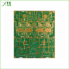
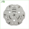
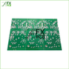
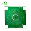
A copper Coin PCB is embedding or inserting a copper block into a specific area of a PCB, and it can also be called an embedded copper coin PCB. Heat-generating electronic components are directly mounted onto the copper block, which utilizes the high thermal conductivity of copper to dissipate heat quickly. Embedded copper coin PCBs not only offer excellent heat dissipation but also save board space, making them increasingly popular in recent years.
TYPES OF COPPER COIN PCB:
Depending on the copper coin PCB process, there are two types of PCBs you will find. These are:
Embedded Copper Coin PCB: It has a copper coin inserted in the PCB slot. The insertion happens after routing, and metallization is done with the PCB press. The copper coin connects with the PCB, thanks to the embedded quality. That’s why the name is as such.
Buried Copper Coin PCB: Builders hide the copper coin in the pre-milling groove. They do so at the time of pressing. A laminated prepreg is used to connect the PCB and copper coin.
Production Process of Embedded Copper Coin PCB
The differences in thermal expansion coefficients, lamination thickness, and other factors between the copper coin and the PCB Material, can lead to depressions in the copper coin, resin overflow, and cracks between the copper coin and resin. So the lamination process for embedded copper coin PCB is more complex than standard PCBs.
The production process begins with the inner layer, the below is the production process of the inner layer of copper coin PCB.
Copper Coin PCB Inner Layer Fabrication
Copper Coin PCB Outer Layer Fabrication
This comprehensive process ensures the high performance and reliability of embedded copper coin PCBs, making them suitable for advanced applications like 5G communication equipment.
As electronic products trend toward being lighter, thinner, and smaller, coupled with the wide usage of high-power electronic components, heat dissipation requirements are increasing. Consequently, finding the optimal solutions for heat dissipation and structural design has become a significant challenge in electronic design.
With the rapid development of next-generation information technology, energy-saving and new-energy vehicles, power equipment, aerospace, and other fields, addressing heat dissipation challenges has become increasingly urgent. Embedded copper coin PCBs, with their high thermal conductivity and excellent heat dissipation capabilities, offer an effective solution to the heat management issues of high-power electronic components in specialized applications.
In addition to their superior heat dissipation properties, embedded copper coin PCBs also save circuit board space, making them highly promising for a wide range of applications.
If you are looking for a PCB manufacturer to produce your copper coin PCB design, please send us your inquiry to FX PCB to get a quote !
Description
What is copper coin PCB?
A copper Coin PCB is embedding or inserting a copper block into a specific area of a PCB, and it can also be called an embedded copper coin PCB. Heat-generating electronic components are directly mounted onto the copper block, which utilizes the high thermal conductivity of copper to dissipate heat quickly. Embedded copper coin PCBs not only offer excellent heat dissipation but also save board space, making them increasingly popular in recent years.
TYPES OF COPPER COIN PCB:
Depending on the copper coin PCB process, there are two types of PCBs you will find. These are:
- Embedded Copper Coin PCB: It has a copper coin inserted in the PCB slot. The insertion happens after routing, and metallization is done with the PCB press. The copper coin connects with the PCB, thanks to the embedded quality. That’s why the name is as such.
- Buried Copper Coin PCB: Builders hide the copper coin in the pre-milling groove. They do so at the time of pressing. A laminated prepreg is used to connect the PCB and copper coin.
Production Process of Embedded Copper Coin PCB
The differences in thermal expansion coefficients, lamination thickness, and other factors between the copper coin and the PCB Material, can lead to depressions in the copper coin, resin overflow, and cracks between the copper coin and resin. So the lamination process for embedded copper coin PCB is more complex than standard PCBs.
The production process begins with the inner layer, the below is the production process of the inner layer of copper coin PCB.
Copper Coin PCB Inner Layer Fabrication
Copper Coin PCB Outer Layer Fabrication
This comprehensive process ensures the high performance and reliability of embedded copper coin PCBs, making them suitable for advanced applications like 5G communication equipment.
As electronic products trend toward being lighter, thinner, and smaller, coupled with the wide usage of high-power electronic components, heat dissipation requirements are increasing. Consequently, finding the optimal solutions for heat dissipation and structural design has become a significant challenge in electronic design.
With the rapid development of next-generation information technology, energy-saving and new-energy vehicles, power equipment, aerospace, and other fields, addressing heat dissipation challenges has become increasingly urgent. Embedded copper coin PCBs, with their high thermal conductivity and excellent heat dissipation capabilities, offer an effective solution to the heat management issues of high-power electronic components in specialized applications.
In addition to their superior heat dissipation properties, embedded copper coin PCBs also save circuit board space, making them highly promising for a wide range of applications.
If you are looking for a PCB manufacturer to produce your copper coin PCB design, please send us your inquiry to FX PCB to get a quote !