Fischer Technology, Inc. EDXRF Instrument for Non-destructive Microstructure Wafer Metrology FISCHERSCOPE® X-RAY XDV®-µ SEMI

Description
The FISCHERSCOPE X-RAY XDV-μ SEMI is an automated measurement system optimized for the quality control of micro-structures in complex 2.5D/3D packaging applications in the semiconductor industry. Fully automated analysis prevents damage to valuable wafer material. And consistent test conditions deliver reliable results. The instrument is suitable for use in clean rooms, and a comprehensive equipment catalog allows simple integration into existing wafer fabs. Features: Fully automated wafer handling and test process enables efficient staff deployment Can precisely test structures up to 10 µm in diameter Automatically locates positions to be measured with image recognition Simple operation via Fischer WinFTM software Individually applicable: manual measurements are possible at any time Flexible: docking station for FOUP, SMIF and cassette, for 6"", 8"" and 12"" wafers Applications: Coating Thickness Measurement Base metallization layers (UBM) on a nanometer scale Thin lead-free solder caps on copper pillars Extremely small contact surfaces and other complex 2.5D/3D packaging applications Material Analysis C4 and smaller solder bumps Lead-free solder caps on copper pillars
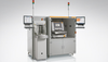
Datasheet
Description
The FISCHERSCOPE X-RAY XDV-μ SEMI is an automated measurement system optimized for the quality control of micro-structures in complex 2.5D/3D packaging applications in the semiconductor industry. Fully automated analysis prevents damage to valuable wafer material. And consistent test conditions deliver reliable results. The instrument is suitable for use in clean rooms, and a comprehensive equipment catalog allows simple integration into existing wafer fabs. Features: Fully automated wafer handling and test process enables efficient staff deployment Can precisely test structures up to 10 µm in diameter Automatically locates positions to be measured with image recognition Simple operation via Fischer WinFTM software Individually applicable: manual measurements are possible at any time Flexible: docking station for FOUP, SMIF and cassette, for 6"", 8"" and 12"" wafers Applications: Coating Thickness Measurement Base metallization layers (UBM) on a nanometer scale Thin lead-free solder caps on copper pillars Extremely small contact surfaces and other complex 2.5D/3D packaging applications Material Analysis C4 and smaller solder bumps Lead-free solder caps on copper pillars
Datasheet

Suppliers

Company
Product
Description
Supplier Links
EDXRF Instrument for Non-destructive Microstructure Wafer Metrology - FISCHERSCOPE® X-RAY XDV®-µ SEMI - Fischer Technology, Inc.
Windsor, CT, USA
EDXRF Instrument for Non-destructive Microstructure Wafer Metrology
FISCHERSCOPE® X-RAY XDV®-µ SEMI
EDXRF Instrument for Non-destructive Microstructure Wafer Metrology FISCHERSCOPE® X-RAY XDV®-µ SEMI
The FISCHERSCOPE X-RAY XDV-μ SEMI is an automated measurement system optimized for the quality control of micro-structures in complex 2.5D/3D packaging applications in the semiconductor industry. Fully automated analysis prevents damage to valuable wafer material. And consistent test conditions deliver reliable results. The instrument is suitable for use in clean rooms, and a comprehensive equipment catalog allows simple integration into existing wafer fabs. Features: Fully automated wafer handling and test process enables efficient staff deployment Can precisely test structures up to 10 µm in diameter Automatically locates positions to be measured with image recognition Simple operation via Fischer WinFTM software Individually applicable: manual measurements are possible at any time Flexible: docking station for FOUP, SMIF and cassette, for 6"", 8"" and 12"" wafers Applications: Coating Thickness Measurement Base metallization layers (UBM) on a nanometer scale Thin lead-free solder caps on copper pillars Extremely small contact surfaces and other complex 2.5D/3D packaging applications Material Analysis C4 and smaller solder bumps Lead-free solder caps on copper pillars

The FISCHERSCOPE X-RAY XDV-μ SEMI is an automated measurement system optimized for the quality control of micro-structures in complex 2.5D/3D packaging applications in the semiconductor industry. Fully automated analysis prevents damage to valuable wafer material. And consistent test conditions deliver reliable results. The instrument is suitable for use in clean rooms, and a comprehensive equipment catalog allows simple integration into existing wafer fabs.

Features:

  • Fully automated wafer handling and test process enables efficient staff deployment
  • Can precisely test structures up to 10 µm in diameter
  • Automatically locates positions to be measured with image recognition
  • Simple operation via Fischer WinFTM software
  • Individually applicable: manual measurements are possible at any time
  • Flexible: docking station for FOUP, SMIF and cassette, for 6"", 8"" and 12"" wafers

Applications:

Coating Thickness Measurement

  • Base metallization layers (UBM) on a nanometer scale
  • Thin lead-free solder caps on copper pillars
  • Extremely small contact surfaces and other complex 2.5D/3D packaging applications

Material Analysis

  • C4 and smaller solder bumps
  • Lead-free solder caps on copper pillars
Supplier's Site Datasheet

Technical Specifications

  Fischer Technology, Inc.
Product Category X-Ray Fluorescence Spectrometers
Product Number FISCHERSCOPE® X-RAY XDV®-µ SEMI
Product Name EDXRF Instrument for Non-destructive Microstructure Wafer Metrology
Special Features Microscope; Cooled Detector; Thickness Testing
Unlock Full Specs
to access all available technical data

Similar Products

JPS-9030 Photoelectron Spectrometer -  - JEOL USA, Inc.
Specs
Detector Type multichannel plate
View Details
Handheld X-ray Fluorescence (XRF) Analyzer, DELTA Classic -  - Evident Scientific
Specs
Detector Type Si-PIN Diode
Excitation Source X-Ray Tubes
Display Digital Meter
View Details
Inline Solution Analyzer - #U600093MasterXRF 4 Level - Au (Gold) - Pratt & Whitney Measurement Systems, Inc.
Specs
ICP Measurement Mode Simultaneous
Detector Type Silicon-drift-detector (SDD)
Excitation Source X-Ray Tubes
View Details