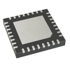
DIODES Incorporated Clock Buffers, Drivers PI6C49S1504TZHIEX

Description
Clock Fanout Buffer (Distribution) IC 3:5 1.5 GHz 32-VFQFN Exposed Pad
Description
Clock Fanout Buffer (Distribution) IC 3:5 1.5 GHz 32-VFQFN Exposed Pad
Datasheet
Datasheet Summary
Powered by GS/AI

The PI6C49S1504TZHIEX is a high-performance selectable 1:4 differential fanout buffer from Quarktwin Technology Ltd. It supports output frequencies of up to 1.5GHz, making it suitable for applications requiring low-jitter clock signal distribution, such as networking systems and high-frequency computing platforms. The device features four differential outputs organized into two banks, with user-configurable output signaling standards including LVDS, LVPECL, or HCSL. It provides an LVCMOS reference output up to 200MHz and has ultra-low additive phase jitter of less than 0.03ps at typical conditions. The device supports selectable reference inputs for single-ended, differential, or crystal sources, and offers low skew between outputs within banks (less than 40ps) and low input-to-output delay (typical less than 1.5ns). The PI6C49S1504TZHIEX operates with a power supply of 2.5V or 3.3V and is designed to function within an industrial temperature range of -40¬8C to 85¬8C. It is packaged in a 32-pin TQFN format and is fully RoHS compliant, making it suitable for environmentally conscious designs.

Datasheet Summary
Powered by GS/AI

The PI6C49S1504TZHIEX is a high-performance selectable 1:4 differential fanout buffer from Quarktwin Technology Ltd. It supports output frequencies of up to 1.5GHz, making it suitable for applications requiring low-jitter clock signal distribution, such as networking systems and high-frequency computing platforms. The device features four differential outputs organized into two banks, with user-configurable output signaling standards including LVDS, LVPECL, or HCSL. It provides an LVCMOS reference output up to 200MHz and has ultra-low additive phase jitter of less than 0.03ps at typical conditions. The device supports selectable reference inputs for single-ended, differential, or crystal sources, and offers low skew between outputs within banks (less than 40ps) and low input-to-output delay (typical less than 1.5ns). The PI6C49S1504TZHIEX operates with a power supply of 2.5V or 3.3V and is designed to function within an industrial temperature range of -40¬8C to 85¬8C. It is packaged in a 32-pin TQFN format and is fully RoHS compliant, making it suitable for environmentally conscious designs.

Suppliers

Company
Product
Description
Supplier Links
Clock Buffers, Drivers - PI6C49S1504TZHIEX - Quarktwin Technology Ltd.
Shenzhen, Guangdong, China
Clock Buffers, Drivers
PI6C49S1504TZHIEX
Clock Buffers, Drivers PI6C49S1504TZHIEX
Clock Fanout Buffer (Distribution) IC 3:5 1.5 GHz 32-VFQFN Exposed Pad

Clock Fanout Buffer (Distribution) IC 3:5 1.5 GHz 32-VFQFN Exposed Pad

Buy Now Datasheet

Technical Specifications

  Quarktwin Technology Ltd.
Product Category Gate Drivers
Product Number PI6C49S1504TZHIEX
Product Name Clock Buffers, Drivers
Output Configuration Inverting
Supply Voltage 2.38 to 3.46 volts
Switching Frequency 1.50E6 kHz
Unlock Full Specs
to access all available technical data

Similar Products

Clock Buffers, Drivers - CDCLVD110VFG4 - Quarktwin Technology Ltd.
Specs
Output Configuration Inverting
Supply Voltage 2.38 to 2.62 volts
Switching Frequency 1.10E6 kHz
View Details
Clock Buffers, Drivers - SI53354BD13636-AMR - Quarktwin Technology Ltd.
Specs
Output Configuration Inverting
Supply Voltage 1.71 to 3.46 volts
Switching Frequency 250000 kHz
View Details
Power Distribution Switches, Load Drivers - A6812EEP-T - Quarktwin Technology Ltd.
Specs
Driver Type High-side
Number of Outputs 20
Output Configuration Inverting; Noninverting
View Details
2 suppliers