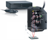
Bruker Corporation Metrology Solutions for Semiconductors

Description
Bruker Semiconductor develops, manufactures, markets, and supports metrology solutions for thin films, which are based on novel, rapid, non-contacting and non-destructive X-ray technology. With Bruker™s acquisition of Jordan Valley Semiconductors, a name synonymous with unparalleled worldwide customer service and support, 75% of the world's top 25 semiconductor manufacturers rely on Bruker metrology tools for front-end and back-end applications, including development of their next-generation thin films. Bruker commitment to innovation and technology leadership drives the continued release of new advancements in metrology, and has garnered numerous awards and industry recognition.  In applications ranging from C-S thin films materials characterization to wafer substrate analysis and defect detection, Bruker™s systems provide simulation analysis and fit. HRXRD, XRR, WA-XRD, and XRDI measurement types are fully supported, enabling researchers, production engineers, and process developers unparalleled capabilities. Whether you are a semi and C-S fabricator, R&D center or academy, or an industry materials research facility, Bruker has a specifically designed solution for your metrology needs.

Suppliers

Company
Product
Description
Supplier Links
Metrology Solutions for Semiconductors -  - Bruker Corporation
Billerica, MA, USA
Metrology Solutions for Semiconductors
Bruker Semiconductor develops, manufactures, markets, and supports metrology solutions for thin films, which are based on novel, rapid, non-contacting and non-destructive X-ray technology. With Bruker™s acquisition of Jordan Valley Semiconductors, a name synonymous with unparalleled worldwide customer service and support, 75% of the world's top 25 semiconductor manufacturers rely on Bruker metrology tools for front-end and back-end applications, including development of their next-generation thin films. Bruker commitment to innovation and technology leadership drives the continued release of new advancements in metrology, and has garnered numerous awards and industry recognition.  In applications ranging from C-S thin films materials characterization to wafer substrate analysis and defect detection, Bruker™s systems provide simulation analysis and fit. HRXRD, XRR, WA-XRD, and XRDI measurement types are fully supported, enabling researchers, production engineers, and process developers unparalleled capabilities. Whether you are a semi and C-S fabricator, R&D center or academy, or an industry materials research facility, Bruker has a specifically designed solution for your metrology needs.

Bruker Semiconductor develops, manufactures, markets, and supports metrology solutions for thin films, which are based on novel, rapid, non-contacting and non-destructive X-ray technology. With Bruker™s acquisition of Jordan Valley Semiconductors, a name synonymous with unparalleled worldwide customer service and support, 75% of the world's top 25 semiconductor manufacturers rely on Bruker metrology tools for front-end and back-end applications, including development of their next-generation thin films. Bruker commitment to innovation and technology leadership drives the continued release of new advancements in metrology, and has garnered numerous awards and industry recognition.
 In applications ranging from C-S thin films materials characterization to wafer substrate analysis and defect detection, Bruker™s systems provide simulation analysis and fit. HRXRD, XRR, WA-XRD, and XRDI measurement types are fully supported, enabling researchers, production engineers, and process developers unparalleled capabilities. Whether you are a semi and C-S fabricator, R&D center or academy, or an industry materials research facility, Bruker has a specifically designed solution for your metrology needs.

Supplier's Site

Technical Specifications

  Bruker Corporation
Product Category Wafer and Thin Film Instrumentation
Product Name Metrology Solutions for Semiconductors
Technology Profilometer or AFM (optional feature); X-ray Diffractometer (optional feature)
Unlock Full Specs
to access all available technical data

Similar Products

Wafer MV - fti-1000-wafer-mv - Cosmic Equipment SpA
Cosmic Equipment SpA
Specs
Form Factor Monitor or instrument
Applications Wafer
View Details
Wafer Edge Grinders - CVP-3000 Series - Daitron Co., Ltd.
Specs
Form Factor Monitor or instrument
Mounting / Loading Floor
Applications Wafer
View Details
EC-52000IC ION CLEANER -  - JEOL USA, Inc.
Specs
Form Factor Monitor or instrument
Mounting / Loading Floor
View Details
Thin Film Monitors - Confocal Laser Sensor - LT-9010M - KEYENCE
Specs
Form Factor Monitor or instrument; Controller; Sensor or sensing element
Mounting / Loading In-process, in-situ or system mounted; In-line; Floor
Technology Confocal
View Details