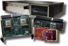

The XC2VP2-6FF672I is a member of the Virtex-II Pro FPGA family, designed for high-performance applications. It features 3,168 logic cells and supports up to 1,408 user I/O pads. The device includes four RocketIO transceiver blocks, enabling high-speed serial communication with baud rates ranging from 600 Mb/s to 3.125 Gb/s. The FPGA is built on SRAM-based technology, allowing for in-system configuration and flexibility in logic resource allocation. This part is equipped with dedicated 18-bit x 18-bit multiplier blocks and a memory hierarchy that includes SelectRAM+ resources, providing efficient data handling capabilities. The XC2VP2-6FF672I also incorporates advanced clock management features, including Digital Clock Managers (DCMs) for precise clock control. The device is packaged in a 672-ball Flip-Chip Fine-Pitch BGA format, suitable for compact designs. Engineers considering this FPGA should evaluate its performance characteristics, including power consumption and I/O capabilities, to determine its suitability for their specific applications.
IC FPGA 204 I/O 672FCBGA
Virtex®-II Pro Field Programmable Gate Array (FPGA) IC 204 221184 3168 672-BBGA, FCBGA
| Lingto Electronic Limited | Quarktwin Technology Ltd. | |
|---|---|---|
| Product Category | Field-Programmable Gate Arrays (FPGA) | Field-Programmable Gate Arrays (FPGA) |
| Product Number | XC2VP2-6FF672I | XC2VP2-6FF672I |
| Product Name | Embedded - FPGAs (Field Programmable Gate Array) | FPGAs (Field Programmable Gate Array) |
| Logic Cells / Logic Blocks | 3168 | 3168 |
| User I/Os | 204 pins | 204 pins |
| Package Type | Other; 672-BBGA, FCBGA |