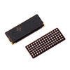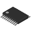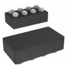
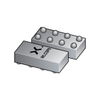
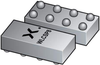
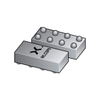
Nexperia B.V. Dual supply translating transceiver; auto direction sensing; 3-state NXB0102UNZ

Description
The NXB0102 is a 2-bit, dual supply translating transceiver with auto direction sensing, that enables bidirectional voltage level translation. It features two 2-bit input-output ports (An and Bn), one output enable input (OE) and two supply pins (VCC(A) and VCC(B)). VCC(A) can be supplied at any voltage between 1.2 V and 3.6 V and VCC(B) can be supplied at any voltage between 1.65 V and 5.5 V, making the device suitable for translating between any of the low voltage nodes (1.2 V, 1.5 V, 1.8 V, 2.5 V, 3.3 V and 5.0 V). Pins An and OE are referenced to VCC(A) and pins Bn are referenced to VCC(B). A LOW level at pin OE causes the outputs to assume a high-impedance OFF-state. This device is fully specified for partial power-down applications using IOFF. The IOFF circuitry disables the output, preventing the damaging backflow current through the device when it is powered down. Features and benefits Wide supply voltage range: VCC(A): 1.2 V to 3.6 V and VCC(B): 1.65 V to 5.5 V IOFF circuitry provides partial Power-down mode operation Inputs accept voltages up to 5.5 V ESD protection: HBM: ANSI/ESDA/JEDEC JS-001 class 2 exceeds 2500 V for A port HBM: ANSI/ESDA/JEDEC JS-001 class 3B exceeds 15000 V for B port CDM: ANSI/ESDA/JEDEC JS-002 class C3 exceeds 1500 V Latch-up performance exceeds 100 mA per JESD 78B Class II Specified from −40 °C to +85 °C and −40 °C to +125 °C
Request a Quote Datasheet
Description
The NXB0102 is a 2-bit, dual supply translating transceiver with auto direction sensing, that enables bidirectional voltage level translation. It features two 2-bit input-output ports (An and Bn), one output enable input (OE) and two supply pins (VCC(A) and VCC(B)). VCC(A) can be supplied at any voltage between 1.2 V and 3.6 V and VCC(B) can be supplied at any voltage between 1.65 V and 5.5 V, making the device suitable for translating between any of the low voltage nodes (1.2 V, 1.5 V, 1.8 V, 2.5 V, 3.3 V and 5.0 V). Pins An and OE are referenced to VCC(A) and pins Bn are referenced to VCC(B). A LOW level at pin OE causes the outputs to assume a high-impedance OFF-state. This device is fully specified for partial power-down applications using IOFF. The IOFF circuitry disables the output, preventing the damaging backflow current through the device when it is powered down. Features and benefits Wide supply voltage range: VCC(A): 1.2 V to 3.6 V and VCC(B): 1.65 V to 5.5 V IOFF circuitry provides partial Power-down mode operation Inputs accept voltages up to 5.5 V ESD protection: HBM: ANSI/ESDA/JEDEC JS-001 class 2 exceeds 2500 V for A port HBM: ANSI/ESDA/JEDEC JS-001 class 3B exceeds 15000 V for B port CDM: ANSI/ESDA/JEDEC JS-002 class C3 exceeds 1500 V Latch-up performance exceeds 100 mA per JESD 78B Class II Specified from −40 °C to +85 °C and −40 °C to +125 °C
Request a Quote Datasheet

Suppliers

Company
Product
Description
Supplier Links
Dual supply translating transceiver; auto direction sensing; 3-state - NXB0102UNZ - Nexperia B.V.
Nijmegen, Netherlands
Dual supply translating transceiver; auto direction sensing; 3-state
NXB0102UNZ
Dual supply translating transceiver; auto direction sensing; 3-state NXB0102UNZ
The NXB0102 is a 2-bit, dual supply translating transceiver with auto direction sensing, that enables bidirectional voltage level translation. It features two 2-bit input-output ports (An and Bn), one output enable input (OE) and two supply pins (VCC(A) and VCC(B)). VCC(A) can be supplied at any voltage between 1.2 V and 3.6 V and VCC(B) can be supplied at any voltage between 1.65 V and 5.5 V, making the device suitable for translating between any of the low voltage nodes (1.2 V, 1.5 V, 1.8 V, 2.5 V, 3.3 V and 5.0 V). Pins An and OE are referenced to VCC(A) and pins Bn are referenced to VCC(B). A LOW level at pin OE causes the outputs to assume a high-impedance OFF-state. This device is fully specified for partial power-down applications using IOFF. The IOFF circuitry disables the output, preventing the damaging backflow current through the device when it is powered down. Features and benefits Wide supply voltage range: VCC(A): 1.2 V to 3.6 V and VCC(B): 1.65 V to 5.5 V IOFF circuitry provides partial Power-down mode operation Inputs accept voltages up to 5.5 V ESD protection: HBM: ANSI/ESDA/JEDEC JS-001 class 2 exceeds 2500 V for A port HBM: ANSI/ESDA/JEDEC JS-001 class 3B exceeds 15000 V for B port CDM: ANSI/ESDA/JEDEC JS-002 class C3 exceeds 1500 V Latch-up performance exceeds 100 mA per JESD 78B Class II Specified from −40 °C to +85 °C and −40 °C to +125 °C

The NXB0102 is a 2-bit, dual supply translating transceiver with auto direction sensing, that enables bidirectional voltage level translation. It features two 2-bit input-output ports (An and Bn), one output enable input (OE) and two supply pins (VCC(A) and VCC(B)). VCC(A) can be supplied at any voltage between 1.2 V and 3.6 V and VCC(B) can be supplied at any voltage between 1.65 V and 5.5 V, making the device suitable for translating between any of the low voltage nodes (1.2 V, 1.5 V, 1.8 V, 2.5 V, 3.3 V and 5.0 V). Pins An and OE are referenced to VCC(A) and pins Bn are referenced to VCC(B). A LOW level at pin OE causes the outputs to assume a high-impedance OFF-state. This device is fully specified for partial power-down applications using IOFF. The IOFF circuitry disables the output, preventing the damaging backflow current through the device when it is powered down.

Features and benefits

  • Wide supply voltage range:
    • VCC(A): 1.2 V to 3.6 V and VCC(B): 1.65 V to 5.5 V
  • IOFF circuitry provides partial Power-down mode operation
  • Inputs accept voltages up to 5.5 V
  • ESD protection:
    • HBM: ANSI/ESDA/JEDEC JS-001 class 2 exceeds 2500 V for A port
    • HBM: ANSI/ESDA/JEDEC JS-001 class 3B exceeds 15000 V for B port
    • CDM: ANSI/ESDA/JEDEC JS-002 class C3 exceeds 1500 V
  • Latch-up performance exceeds 100 mA per JESD 78B Class II
  • Specified from −40 °C to +85 °C and −40 °C to +125 °C
Supplier's Site Datasheet
Translators, Level Shifters - 1727-NXB0102UNZTR-ND - DigiKey
Thief River Falls, MN, United States
Translators, Level Shifters
1727-NXB0102UNZTR-ND
Translators, Level Shifters 1727-NXB0102UNZTR-ND
Voltage Level Translator Bidirectional 1 Circuit 2 Channel 100Mbps 8-WLCSP (0.75x1.55)

Voltage Level Translator Bidirectional 1 Circuit 2 Channel 100Mbps 8-WLCSP (0.75x1.55)

Buy Now Datasheet
Translators, Level Shifters - 1727-NXB0102UNZCT-ND - DigiKey
Thief River Falls, MN, United States
Translators, Level Shifters
1727-NXB0102UNZCT-ND
Translators, Level Shifters 1727-NXB0102UNZCT-ND
Voltage Level Translator Bidirectional 1 Circuit 2 Channel 100Mbps 8-WLCSP (0.75x1.55)

Voltage Level Translator Bidirectional 1 Circuit 2 Channel 100Mbps 8-WLCSP (0.75x1.55)

Buy Now Datasheet
Logic - Translators, Level Shifters - NXB0102UNZ - Lingto Electronic Limited
Shenzhen, China
Logic - Translators, Level Shifters
NXB0102UNZ
Logic - Translators, Level Shifters NXB0102UNZ
NXB0102UN/SOT8023/WL CSP8

NXB0102UN/SOT8023/WLCSP8

Supplier's Site Datasheet
Transceiver, Translating, -40 To 125Degc Rohs Compliant Nexperia - 62AJ8874 - Newark, An Avnet Company
Chicago, IL, United States
Transceiver, Translating, -40 To 125Degc Rohs Compliant Nexperia
62AJ8874
Transceiver, Translating, -40 To 125Degc Rohs Compliant Nexperia 62AJ8874
TRANSCEIVER, TRANSLATING, -40 TO 125DEGC ROHS COMPLIANT: YES

TRANSCEIVER, TRANSLATING, -40 TO 125DEGC ROHS COMPLIANT: YES

Supplier's Site
Integrated Circuits (ICs) - Logic - Translators, Level Shifters - NXB0102UNZ - Acme Chip Technology Co., Limited
Shenzhen, China
Integrated Circuits (ICs) - Logic - Translators, Level Shifters
NXB0102UNZ
Integrated Circuits (ICs) - Logic - Translators, Level Shifters NXB0102UNZ
IC TRANSLTR BIDIRECTIONAL 8WLCSP

IC TRANSLTR BIDIRECTIONAL 8WLCSP

Supplier's Site
Translators, Level Shifters - NXB0102UNZ - Quarktwin Technology Ltd.
Shenzhen, Guangdong, China
Translators, Level Shifters
NXB0102UNZ
Translators, Level Shifters NXB0102UNZ
Voltage Level Translator Bidirectional 1 Circuit 2 Channel 100Mbps 8-WLCSP (0.75x1.55)

Voltage Level Translator Bidirectional 1 Circuit 2 Channel 100Mbps 8-WLCSP (0.75x1.55)

Buy Now Datasheet

Technical Specifications

  Nexperia B.V. DigiKey Lingto Electronic Limited Newark, An Avnet Company Acme Chip Technology Co., Limited Quarktwin Technology Ltd.
Product Category Logic Level Translators Logic Level Translators Logic Level Translators Logic Level Translators Logic Level Translators Logic Level Translators
Product Number NXB0102UNZ 1727-NXB0102UNZTR-ND NXB0102UNZ 62AJ8874 NXB0102UNZ NXB0102UNZ
Product Name Dual supply translating transceiver; auto direction sensing; 3-state Translators, Level Shifters Logic - Translators, Level Shifters Transceiver, Translating, -40 To 125Degc Rohs Compliant Nexperia Integrated Circuits (ICs) - Logic - Translators, Level Shifters Translators, Level Shifters
Logic Family CMOS
Package Type WLCSP8 (SOT8023-1) 8-UFBGA, WLCSP BGA; 8-UFBGA, WLCSP BGA; 8-UFBGA, WLCSP
Features RoHS; ESD Protection RoHS RoHS
Input Voltage 1.2 to 3.6 volts
Unlock Full Specs
to access all available technical data

Similar Products

SIM card interface level translator - NXT4556AURZ - Nexperia B.V.
Specs
Logic Family CMOS
Package Type SOT8057-1
Features RoHS; ESD Protection
View Details
2 suppliers
 - 74AUP1T14GWH - Rochester Electronics
Nexperia B.V.
Specs
Package Type SOT353
Features RoHS
View Details
Logic - Translators, Level Shifters - 74AVC4T245BZX - Lingto Electronic Limited
Specs
Translation Both
View Details
2 suppliers
4-bit dual-supply voltage level translating buffer with Schmitt-trigger; 3-state - NXU0304GU12X - Nexperia B.V.
Specs
Package Type SOT1174-1
Output Type 3-State
Features RoHS; ESD Protection
View Details
2 suppliers