NGD31251 is a high-frequency, dual channel, non-isolation MOSFET gate driver for high power automotive application.
NGD31251 has typical 5 A sink and 5 A source drive current and it can handle -10 V on its input pins, which improves robustness in systems with moderate ground bouncing. The inputs are independent of supply voltage and can be connected to most controller outputs.
NGD31251 has 11 ns rising and 13 ns falling propagation delay which allows the systems operating at high frequency with less delay matching variations. These delays are very suited for applications requiring dual-gate drivers with critical timing, such as synchronous rectifiers. When connecting two channels in parallel to increase current-drive capability, delay matching between 2 channels (2 ns) is used to avoid shoot through current without adding external series resistor.
Features and benefits
Absolute maximum VDD pin voltage: 28 V
Typical 5 A sink and 5 A source output currents
Input pins capable of withstanding up to -10 V and are independent of power supply
Operation switching frequency up to 1 MHz
VDD UVLO point: 4.2 V
Symmetrical undervoltage lockout for both channels
-40 °C to 140 °C junction temperature range
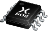
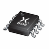
SOT96-2 package
Applications
Power supplies for telecom, datacom and industrial inverters
Power factor correction (PFC) circuits
Solar power supplies
Residential EV chargers
Motor drives
Pulse transformer drivers
Figure 1. Application for synchronous rectification
NGD31251 is a high-frequency, dual channel, non-isolation MOSFET gate driver for high power automotive application.
NGD31251 has typical 5 A sink and 5 A source drive current and it can handle -10 V on its input pins, which improves robustness in systems with moderate ground bouncing. The inputs are independent of supply voltage and can be connected to most controller outputs.
NGD31251 has 11 ns rising and 13 ns falling propagation delay which allows the systems operating at high frequency with less delay matching variations. These delays are very suited for applications requiring dual-gate drivers with critical timing, such as synchronous rectifiers. When connecting two channels in parallel to increase current-drive capability, delay matching between 2 channels (2 ns) is used to avoid shoot through current without adding external series resistor.
Features and benefits
- Absolute maximum VDD pin voltage: 28 V
- Typical 5 A sink and 5 A source output currents
- Input pins capable of withstanding up to -10 V and are independent of power supply
- Operation switching frequency up to 1 MHz
- VDD UVLO point: 4.2 V
- Symmetrical undervoltage lockout for both channels
- -40 °C to 140 °C junction temperature range
- SOT96-2 package
Applications
- Power supplies for telecom, datacom and industrial inverters
- Power factor correction (PFC) circuits
- Solar power supplies
- Residential EV chargers
- Motor drives
- Pulse transformer drivers
Figure 1. Application for synchronous rectification