Nexperia B.V. 20 V, P-channel Trench MOSFET BUK4D122-20PX

Description
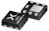
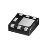
P-channel enhancement mode Field-Effect Transistor (FET) in a leadless medium power DFN2020MD-6 (SOT1220) Surface-Mounted Device (SMD) plastic package using Trench MOSFET technology. Features and benefits Extended temperature range Tj = 175 °C Small and leadless ultra thin SMD plastic package: 2 x 2 x 0.65 mm Tin-plated 100% solderable side pads for optical solder inspection ElectroStatic Discharge (ESD) protection > 2 kV HBM Trench MOSFET technology AEC-Q101 qualified Applications Relay driver High-speed line driver High-side loadswitch Switching circuits
Request a Quote Datasheet
Description
P-channel enhancement mode Field-Effect Transistor (FET) in a leadless medium power DFN2020MD-6 (SOT1220) Surface-Mounted Device (SMD) plastic package using Trench MOSFET technology. Features and benefits Extended temperature range Tj = 175 °C Small and leadless ultra thin SMD plastic package: 2 x 2 x 0.65 mm Tin-plated 100% solderable side pads for optical solder inspection ElectroStatic Discharge (ESD) protection > 2 kV HBM Trench MOSFET technology AEC-Q101 qualified Applications Relay driver High-speed line driver High-side loadswitch Switching circuits
Request a Quote Datasheet

Suppliers

Company
Product
Description
Supplier Links
20 V, P-channel Trench MOSFET - BUK4D122-20PX - Nexperia B.V.
Nijmegen, Netherlands
20 V, P-channel Trench MOSFET
BUK4D122-20PX
20 V, P-channel Trench MOSFET BUK4D122-20PX
P-channel enhancement mode Field-Effect Transistor (FET) in a leadless medium power DFN2020MD-6 (SOT1220) Surface-Mounted Device (SMD) plastic package using Trench MOSFET technology. Features and benefits Extended temperature range Tj = 175 °C Small and leadless ultra thin SMD plastic package: 2 x 2 x 0.65 mm Tin-plated 100% solderable side pads for optical solder inspection ElectroStatic Discharge (ESD) protection > 2 kV HBM Trench MOSFET technology AEC-Q101 qualified Applications Relay driver High-speed line driver High-side loadswitch Switching circuits

P-channel enhancement mode Field-Effect Transistor (FET) in a leadless medium power DFN2020MD-6 (SOT1220) Surface-Mounted Device (SMD) plastic package using Trench MOSFET technology.

Features and benefits

  • Extended temperature range Tj = 175 °C
  • Small and leadless ultra thin SMD plastic package: 2 x 2 x 0.65 mm
  • Tin-plated 100% solderable side pads for optical solder inspection
  • ElectroStatic Discharge (ESD) protection > 2 kV HBM
  • Trench MOSFET technology
  • AEC-Q101 qualified

Applications

  • Relay driver
  • High-speed line driver
  • High-side loadswitch
  • Switching circuits
Supplier's Site Datasheet
Single FETs, MOSFETs - 1727-BUK4D122-20PX-ND - DigiKey
Thief River Falls, MN, United States
Single FETs, MOSFETs
1727-BUK4D122-20PX-ND
Single FETs, MOSFETs 1727-BUK4D122-20PX-ND
BUK4D122-20PX

BUK4D122-20PX

Buy Now Datasheet

Technical Specifications

  Nexperia B.V. DigiKey
Product Category Metal-Oxide Semiconductor FET (MOSFET) Transistors
Product Number BUK4D122-20PX 1727-BUK4D122-20PX-ND
Product Name 20 V, P-channel Trench MOSFET Single FETs, MOSFETs
MOSFET Operating Mode Enhancement
V(BR)DSS -20 volts
IDSS -3200 milliamps
VGS(off) 8 volts
Unlock Full Specs
to access all available technical data
