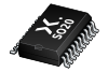
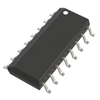
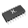
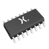
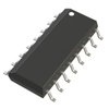
Nexperia B.V. 8-bit serial-in/serial-out or parallel-out shift register with output latches 74VHCT595D-Q100J

Description
The 74VHC595-Q100; 74VHCT595-Q100 are high-speed Si-gate CMOS devices and are pin compatible with Low-power Schottky TTL (LSTTL). It is specified in compliance with JEDEC standard No. 7A. The 74VHC595-Q100; 74VHCT595-Q100 are 8-stage serial shift registers with a storage register and 3-state outputs. The shift registers have separate clocks. Data is shifted on the positive-going transitions of the shift register clock input (SHCP). The data in each register is transferred to the storage register on a positive-going transition of the storage register clock input (STCP). If both clocks are connected together, the shift register will always be one clock pulse ahead of the storage register. The shift register has a serial input (DS) and a serial standard output (Q7S) for cascading. It is also provided with asynchronous reset (active LOW) for all 8 shift register stages. The storage register has 8 parallel 3-state bus driver outputs. Data in the storage register appears at the output whenever the output enable input (OE) is LOW. This product has been qualified to the Automotive Electronics Council (AEC) standard Q100 (Grade 1) and is suitable for use in automotive applications. Features and benefits Automotive product qualification in accordance with AEC-Q100 (Grade 1) Specified from -40 °C to +85 °C and from -40 °C to +125 °C Balanced propagation delays All inputs have Schmitt-trigger action Inputs accept voltages higher than VCC Input levels: For 74VHC595-Q100: CMOS level For 74VHCT595-Q100: TTL level ESD protection: HBM: ANSI/ESDA/JEDEC JS-001 class 2 exceeds 2000 V CDM: ANSI/ESDA/JEDEC JS-002 class C3 exceeds 1000 V Multiple package options DHVQFN package with Side-Wettable Flanks enabling Automated Optical Inspection (AOI) of solder joints Applications Serial-to-parallel data conversion Remote control holding register
Request a Quote Datasheet
Description
The 74VHC595-Q100; 74VHCT595-Q100 are high-speed Si-gate CMOS devices and are pin compatible with Low-power Schottky TTL (LSTTL). It is specified in compliance with JEDEC standard No. 7A. The 74VHC595-Q100; 74VHCT595-Q100 are 8-stage serial shift registers with a storage register and 3-state outputs. The shift registers have separate clocks. Data is shifted on the positive-going transitions of the shift register clock input (SHCP). The data in each register is transferred to the storage register on a positive-going transition of the storage register clock input (STCP). If both clocks are connected together, the shift register will always be one clock pulse ahead of the storage register. The shift register has a serial input (DS) and a serial standard output (Q7S) for cascading. It is also provided with asynchronous reset (active LOW) for all 8 shift register stages. The storage register has 8 parallel 3-state bus driver outputs. Data in the storage register appears at the output whenever the output enable input (OE) is LOW. This product has been qualified to the Automotive Electronics Council (AEC) standard Q100 (Grade 1) and is suitable for use in automotive applications. Features and benefits Automotive product qualification in accordance with AEC-Q100 (Grade 1) Specified from -40 °C to +85 °C and from -40 °C to +125 °C Balanced propagation delays All inputs have Schmitt-trigger action Inputs accept voltages higher than VCC Input levels: For 74VHC595-Q100: CMOS level For 74VHCT595-Q100: TTL level ESD protection: HBM: ANSI/ESDA/JEDEC JS-001 class 2 exceeds 2000 V CDM: ANSI/ESDA/JEDEC JS-002 class C3 exceeds 1000 V Multiple package options DHVQFN package with Side-Wettable Flanks enabling Automated Optical Inspection (AOI) of solder joints Applications Serial-to-parallel data conversion Remote control holding register
Request a Quote Datasheet

Suppliers

Company
Product
Description
Supplier Links
8-bit serial-in/serial-out or parallel-out shift register with output latches - 74VHCT595D-Q100J - Nexperia B.V.
Nijmegen, Netherlands
8-bit serial-in/serial-out or parallel-out shift register with output latches
74VHCT595D-Q100J
8-bit serial-in/serial-out or parallel-out shift register with output latches 74VHCT595D-Q100J
The 74VHC595-Q100; 74VHCT595-Q100 are high-speed Si-gate CMOS devices and are pin compatible with Low-power Schottky TTL (LSTTL). It is specified in compliance with JEDEC standard No. 7A. The 74VHC595-Q100; 74VHCT595-Q100 are 8-stage serial shift registers with a storage register and 3-state outputs. The shift registers have separate clocks. Data is shifted on the positive-going transitions of the shift register clock input (SHCP). The data in each register is transferred to the storage register on a positive-going transition of the storage register clock input (STCP). If both clocks are connected together, the shift register will always be one clock pulse ahead of the storage register. The shift register has a serial input (DS) and a serial standard output (Q7S) for cascading. It is also provided with asynchronous reset (active LOW) for all 8 shift register stages. The storage register has 8 parallel 3-state bus driver outputs. Data in the storage register appears at the output whenever the output enable input (OE) is LOW. This product has been qualified to the Automotive Electronics Council (AEC) standard Q100 (Grade 1) and is suitable for use in automotive applications. Features and benefits Automotive product qualification in accordance with AEC-Q100 (Grade 1) Specified from -40 °C to +85 °C and from -40 °C to +125 °C Balanced propagation delays All inputs have Schmitt-trigger action Inputs accept voltages higher than VCC Input levels: For 74VHC595-Q100: CMOS level For 74VHCT595-Q100: TTL level ESD protection: HBM: ANSI/ESDA/JEDEC JS-001 class 2 exceeds 2000 V CDM: ANSI/ESDA/JEDEC JS-002 class C3 exceeds 1000 V Multiple package options DHVQFN package with Side-Wettable Flanks enabling Automated Optical Inspection (AOI) of solder joints Applications Serial-to-parallel data conversion Remote control holding register

The 74VHC595-Q100; 74VHCT595-Q100 are high-speed Si-gate CMOS devices and are pin compatible with Low-power Schottky TTL (LSTTL). It is specified in compliance with JEDEC standard No. 7A.

The 74VHC595-Q100; 74VHCT595-Q100 are 8-stage serial shift registers with a storage register and 3-state outputs. The shift registers have separate clocks.

Data is shifted on the positive-going transitions of the shift register clock input (SHCP). The data in each register is transferred to the storage register on a positive-going transition of the storage register clock input (STCP). If both clocks are connected together, the shift register will always be one clock pulse ahead of the storage register.

The shift register has a serial input (DS) and a serial standard output (Q7S) for cascading. It is also provided with asynchronous reset (active LOW) for all 8 shift register stages. The storage register has 8 parallel 3-state bus driver outputs. Data in the storage register appears at the output whenever the output enable input (OE) is LOW.

This product has been qualified to the Automotive Electronics Council (AEC) standard Q100 (Grade 1) and is suitable for use in automotive applications.

Features and benefits

  • Automotive product qualification in accordance with AEC-Q100 (Grade 1)
    • Specified from -40 °C to +85 °C and from -40 °C to +125 °C
  • Balanced propagation delays
  • All inputs have Schmitt-trigger action
  • Inputs accept voltages higher than VCC
  • Input levels:
    • For 74VHC595-Q100: CMOS level
    • For 74VHCT595-Q100: TTL level
  • ESD protection:
    • HBM: ANSI/ESDA/JEDEC JS-001 class 2 exceeds 2000 V
    • CDM: ANSI/ESDA/JEDEC JS-002 class C3 exceeds 1000 V
  • Multiple package options
  • DHVQFN package with Side-Wettable Flanks enabling Automated Optical Inspection (AOI) of solder joints

Applications

  • Serial-to-parallel data conversion
  • Remote control holding register
Supplier's Site Datasheet
Shift Registers - 1727-74VHCT595D-Q100JTR-ND - DigiKey
Thief River Falls, MN, United States
Shift Shift Register 1 Element 8 Bit 16-SO

Shift Shift Register 1 Element 8 Bit 16-SO

Buy Now Datasheet
Logic - Shift Registers - 74VHCT595D-Q100J - Lingto Electronic Limited
Shenzhen, China
Logic - Shift Registers
74VHCT595D-Q100J
Logic - Shift Registers 74VHCT595D-Q100J
IC SHIFT REG 8BIT SISO 16SOIC

IC SHIFT REG 8BIT SISO 16SOIC

Supplier's Site Datasheet
Integrated Circuits (ICs) - Logic - Shift Registers - 74VHCT595D-Q100J - Shenzhen Shengyu Electronics Technology Limited
Futian, China
Integrated Circuits (ICs) - Logic - Shift Registers
74VHCT595D-Q100J
Integrated Circuits (ICs) - Logic - Shift Registers 74VHCT595D-Q100J
IC SHIFT REG 8BIT SISO 16SOIC

IC SHIFT REG 8BIT SISO 16SOIC

Supplier's Site
Shift Registers - 74VHCT595D-Q100J - Quarktwin Technology Ltd.
Shenzhen, Guangdong, China
Shift Registers
74VHCT595D-Q100J
Shift Registers 74VHCT595D-Q100J
Shift Shift Register 1 Element 8 Bit 16-SO

Shift Shift Register 1 Element 8 Bit 16-SO

Buy Now Datasheet

Technical Specifications

  Nexperia B.V. DigiKey Lingto Electronic Limited Shenzhen Shengyu Electronics Technology Limited Quarktwin Technology Ltd.
Product Category Shift Registers Shift Registers Shift Registers Shift Registers Shift Registers
Product Number 74VHCT595D-Q100J 1727-74VHCT595D-Q100JTR-ND 74VHCT595D-Q100J 74VHCT595D-Q100J 74VHCT595D-Q100J
Product Name 8-bit serial-in/serial-out or parallel-out shift register with output latches Shift Registers Logic - Shift Registers Integrated Circuits (ICs) - Logic - Shift Registers Shift Registers
Register Type Serial In / Serial Out - Shift Right Serial In / Parallel Out Serial In / Parallel Out Serial In / Parallel Out
Supply Voltage +7.0 4.5V ~ 5.5V 4.5V ~ 5.5V
Features ESD Protection
Package Type Other; SOT109-1 SOT109-1 SOIC; Other; "16-SOIC (0.154"", 3.90mm Width)" SOIC; Other; 16-SOIC (0.154\", 3.90mm Width)
Unlock Full Specs
to access all available technical data

Similar Products

Logic - Logic - Translators, Level Shifters - 74AVCH2T45GT,115 - 765267-74AVCH2T45GT,115 - Win Source Electronics
Specs
Output Characteristics Tri-State, Non-Inverted
Operating Temperature -40 to 125 C (-40 to 257 F)
View Details
8-bit shift register with output register - 74LVC594APW-Q100J - Nexperia B.V.
Specs
Supply Voltage +6.5
Features ESD Protection
Package Type Other; SOT403-1 SOT403-1
View Details
6 suppliers
Logic - Logic - Translators, Level Shifters - 74AVCH1T45GM,115 - 1007865-74AVCH1T45GM,115 - Win Source Electronics
Specs
Output Characteristics Tri-State, Non-Inverted
Package Type Other; 6-XSON, SOT886 (1.45x1)
Operating Temperature -40 to 125 C (-40 to 257 F)
View Details
8-bit parallel-in/serial out shift register - 74HCT165BZX - Nexperia B.V.
Specs
Register Type Parallel In / Serial Out
Supply Voltage +7
Features ESD Protection
View Details
2 suppliers