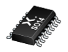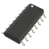
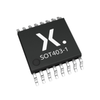
Nexperia B.V. 8-stage shift-and-store bus register 74HCT4094PWJ

Description
The 74HC4094; 74HCT4094 is an 8-bit serial-in/serial or parallel-out shift register with a storage register and 3-state outputs. Both the shift and storage register have separate clocks. The device features a serial input (D) and two serial outputs (QS1 and QS2) to enable cascading. Data is shifted on the LOW-to-HIGH transitions of the CP input. Data is available at QS1 on the LOW-to-HIGH transitions of the CP input to allow cascading when clock edges are fast. The same data is available at QS2 on the next HIGH-to-LOW transition of the CP input to allow cascading when clock edges are slow. The data in the shift register is transferred to the storage register when the STR input is HIGH. Data in the storage register appears at the outputs whenever the output enable input (OE) is HIGH. A LOW on OE causes the outputs to assume a high-impedance OFF-state. Operation of the OE input does not affect the state of the registers. Inputs include clamp diodes. This enables the use of current limiting resistors to interface inputs to voltages in excess of VCC. Features and benefits Complies with JEDEC standard JESD7A Input levels: For 74HC4094: CMOS level For 74HCT4094: TTL level Low-power dissipation ESD protection: HBM: ANSI/ESDA/JEDEC JS-001 class 2 exceeds 2000 V CDM: ANSI/ESDA/JEDEC JS-002 class C3 exceeds 1000 V Specified from -40 °C to +85 °C and from -40 °C to +125 °C Applications Serial-to-parallel data conversion Remote control holding register
Request a Quote Datasheet
Description
The 74HC4094; 74HCT4094 is an 8-bit serial-in/serial or parallel-out shift register with a storage register and 3-state outputs. Both the shift and storage register have separate clocks. The device features a serial input (D) and two serial outputs (QS1 and QS2) to enable cascading. Data is shifted on the LOW-to-HIGH transitions of the CP input. Data is available at QS1 on the LOW-to-HIGH transitions of the CP input to allow cascading when clock edges are fast. The same data is available at QS2 on the next HIGH-to-LOW transition of the CP input to allow cascading when clock edges are slow. The data in the shift register is transferred to the storage register when the STR input is HIGH. Data in the storage register appears at the outputs whenever the output enable input (OE) is HIGH. A LOW on OE causes the outputs to assume a high-impedance OFF-state. Operation of the OE input does not affect the state of the registers. Inputs include clamp diodes. This enables the use of current limiting resistors to interface inputs to voltages in excess of VCC. Features and benefits Complies with JEDEC standard JESD7A Input levels: For 74HC4094: CMOS level For 74HCT4094: TTL level Low-power dissipation ESD protection: HBM: ANSI/ESDA/JEDEC JS-001 class 2 exceeds 2000 V CDM: ANSI/ESDA/JEDEC JS-002 class C3 exceeds 1000 V Specified from -40 °C to +85 °C and from -40 °C to +125 °C Applications Serial-to-parallel data conversion Remote control holding register
Request a Quote Datasheet

Suppliers

Company
Product
Description
Supplier Links
8-stage shift-and-store bus register - 74HCT4094PWJ - Nexperia B.V.
Nijmegen, Netherlands
8-stage shift-and-store bus register
74HCT4094PWJ
8-stage shift-and-store bus register 74HCT4094PWJ
The 74HC4094; 74HCT4094 is an 8-bit serial-in/serial or parallel-out shift register with a storage register and 3-state outputs. Both the shift and storage register have separate clocks. The device features a serial input (D) and two serial outputs (QS1 and QS2) to enable cascading. Data is shifted on the LOW-to-HIGH transitions of the CP input. Data is available at QS1 on the LOW-to-HIGH transitions of the CP input to allow cascading when clock edges are fast. The same data is available at QS2 on the next HIGH-to-LOW transition of the CP input to allow cascading when clock edges are slow. The data in the shift register is transferred to the storage register when the STR input is HIGH. Data in the storage register appears at the outputs whenever the output enable input (OE) is HIGH. A LOW on OE causes the outputs to assume a high-impedance OFF-state. Operation of the OE input does not affect the state of the registers. Inputs include clamp diodes. This enables the use of current limiting resistors to interface inputs to voltages in excess of VCC. Features and benefits Complies with JEDEC standard JESD7A Input levels: For 74HC4094: CMOS level For 74HCT4094: TTL level Low-power dissipation ESD protection: HBM: ANSI/ESDA/JEDEC JS-001 class 2 exceeds 2000 V CDM: ANSI/ESDA/JEDEC JS-002 class C3 exceeds 1000 V Specified from -40 °C to +85 °C and from -40 °C to +125 °C Applications Serial-to-parallel data conversion Remote control holding register

The 74HC4094; 74HCT4094 is an 8-bit serial-in/serial or parallel-out shift register with a storage register and 3-state outputs. Both the shift and storage register have separate clocks. The device features a serial input (D) and two serial outputs (QS1 and QS2) to enable cascading. Data is shifted on the LOW-to-HIGH transitions of the CP input. Data is available at QS1 on the LOW-to-HIGH transitions of the CP input to allow cascading when clock edges are fast. The same data is available at QS2 on the next HIGH-to-LOW transition of the CP input to allow cascading when clock edges are slow. The data in the shift register is transferred to the storage register when the STR input is HIGH. Data in the storage register appears at the outputs whenever the output enable input (OE) is HIGH. A LOW on OE causes the outputs to assume a high-impedance OFF-state. Operation of the OE input does not affect the state of the registers. Inputs include clamp diodes. This enables the use of current limiting resistors to interface inputs to voltages in excess of VCC.

Features and benefits

  • Complies with JEDEC standard JESD7A
  • Input levels:
    • For 74HC4094: CMOS level
    • For 74HCT4094: TTL level
  • Low-power dissipation
  • ESD protection:
    • HBM: ANSI/ESDA/JEDEC JS-001 class 2 exceeds 2000 V
    • CDM: ANSI/ESDA/JEDEC JS-002 class C3 exceeds 1000 V
  • Specified from -40 °C to +85 °C and from -40 °C to +125 °C

Applications

  • Serial-to-parallel data conversion
  • Remote control holding register
Supplier's Site Datasheet
Shift Registers - 1727-74HCT4094PWJTR-ND - DigiKey
Thief River Falls, MN, United States
Shift Registers
1727-74HCT4094PWJTR-ND
Shift Registers 1727-74HCT4094PWJTR-ND
Shift Shift Register 1 Element 8 Bit 16-TSSOP

Shift Shift Register 1 Element 8 Bit 16-TSSOP

Buy Now Datasheet
Shift Registers - 1727-74HCT4094PWJCT-ND - DigiKey
Thief River Falls, MN, United States
Shift Registers
1727-74HCT4094PWJCT-ND
Shift Registers 1727-74HCT4094PWJCT-ND
Shift Shift Register 1 Element 8 Bit 16-TSSOP

Shift Shift Register 1 Element 8 Bit 16-TSSOP

Buy Now Datasheet
Shift Registers - 1727-74HCT4094PWJDKR-ND - DigiKey
Thief River Falls, MN, United States
Shift Shift Register 1 Element 8 Bit 16-TSSOP

Shift Shift Register 1 Element 8 Bit 16-TSSOP

Buy Now Datasheet
Shift Registers - 74HCT4094PWJ - Quarktwin Technology Ltd.
Shenzhen, Guangdong, China
Shift Registers
74HCT4094PWJ
Shift Registers 74HCT4094PWJ
Shift Shift Register 1 Element 8 Bit 16-TSSOP

Shift Shift Register 1 Element 8 Bit 16-TSSOP

Buy Now Datasheet
Shift Register, 8Bit, -40 To 125Deg C Rohs Compliant Nexperia - 25AK1982 - Newark, An Avnet Company
Chicago, IL, United States
Shift Register, 8Bit, -40 To 125Deg C Rohs Compliant Nexperia
25AK1982
Shift Register, 8Bit, -40 To 125Deg C Rohs Compliant Nexperia 25AK1982
SHIFT REGISTER, 8BIT, -40 TO 125DEG C ROHS COMPLIANT: YES

SHIFT REGISTER, 8BIT, -40 TO 125DEG C ROHS COMPLIANT: YES

Supplier's Site
Logic - Shift Registers - 74HCT4094PWJ - Lingto Electronic Limited
Shenzhen, China
Logic - Shift Registers
74HCT4094PWJ
Logic - Shift Registers 74HCT4094PWJ
IC 8STAGE SHIFT/STORE BUS 16TSSO

IC 8STAGE SHIFT/STORE BUS 16TSSO

Supplier's Site Datasheet
Integrated Circuits (ICs) - Logic - Shift Registers - 74HCT4094PWJ - Acme Chip Technology Co., Limited
Shenzhen, China
Integrated Circuits (ICs) - Logic - Shift Registers
74HCT4094PWJ
Integrated Circuits (ICs) - Logic - Shift Registers 74HCT4094PWJ
IC 8STAGE SHIFT/STORE BUS 16TSSO

IC 8STAGE SHIFT/STORE BUS 16TSSO

Supplier's Site

Technical Specifications

  Nexperia B.V. DigiKey Quarktwin Technology Ltd. Newark, An Avnet Company Lingto Electronic Limited Acme Chip Technology Co., Limited
Product Category Shift Registers Shift Registers Shift Registers Shift Registers Shift Registers Shift Registers
Product Number 74HCT4094PWJ 1727-74HCT4094PWJTR-ND 74HCT4094PWJ 25AK1982 74HCT4094PWJ 74HCT4094PWJ
Product Name 8-stage shift-and-store bus register Shift Registers Shift Registers Shift Register, 8Bit, -40 To 125Deg C Rohs Compliant Nexperia Logic - Shift Registers Integrated Circuits (ICs) - Logic - Shift Registers
Supply Voltage +7 4.5V ~ 5.5V 4.5V ~ 5.5V
Features ESD Protection
Package Type Other; SOT403-1 SOT403-1 TSSOP; Other; "16-TSSOP (0.173"", 4.40mm Width)" SOP; SSOP; TSSOP; Other; 16-TSSOP (0.173\", 4.40mm Width) SSOP; TSSOP; Other; 16-TSSOP (0.173, 4.40mm Width)
Register Type Serial In / Parallel Out Serial In / Parallel Out Serial In / Parallel Out
Unlock Full Specs
to access all available technical data

Similar Products

8-bit parallel-in/serial out shift register - 74HCT166D,653 - Nexperia B.V.
Specs
Register Type Parallel In / Serial Out
Supply Voltage +7
Features ESD Protection
View Details
5 suppliers
Shift Registers - 1727-2217-2-ND - DigiKey
Specs
Register Type Serial In / Parallel Out
Supply Voltage 4.5V ~ 5.5V
Output Characteristics Open-drain
View Details
6 suppliers
Shift Registers - 74HCT164PW/S400J - Quarktwin Technology Ltd.
Specs
Register Type Serial In / Parallel Out
Supply Voltage 4.5V ~ 5.5V
Output Characteristics Push-Pull
View Details
 - 74ALVCH16501DGGS - Rochester Electronics
Nexperia B.V.
Specs
Package Type SOP; SSOP; TSSOP; Other; TSSOP56
Logic Family CMOS
View Details