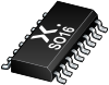
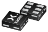
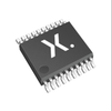
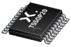
The 74HC75-Q100 is a quad bistable transparent latch with complementary outputs. Two latches are simultaneously controlled by one of two active HIGH enable inputs (LE12 and LE34). When LEnn is HIGH, the data enters the latches and appears at the nQ outputs. The nQ outputs follow the data inputs (nD) as long as LEnn is HIGH (transparent). The data on the nD inputs one set-up time prior to the HIGH-to-LOW transition of the LEnn will be stored in the latches. The latched outputs remain stable as long as the LEnn is LOW. Inputs include clamp diodes. This enables the use of current limiting resistors to interface inputs to voltages in excess of VCC.
This product has been qualified to the Automotive Electronics Council (AEC) standard Q100 (Grade 1) and is suitable for use in automotive applications.
Features and benefits
Automotive product qualification in accordance with AEC-Q100 (Grade 1)
Specified from -40 °C to +85 °C and from -40 °C to +125 °C
Wide supply voltage range from 2.0 V to 6.0 V
CMOS low power dissipation
High noise immunity
Latch-up performance exceeds 100 mA per JESD 78 Class II Level B
Complies with JEDEC standards:
JESD8C (2.7 V to 3.6 V)
JESD7A (2.0 V to 6.0 V)
Complementary Q and Q outputs
VCC and GND on the center pins
CMOS input levels
ESD protection:
HBM: ANSI/ESDA/JEDEC JS-001 class 2 exceeds 2000 V
CDM: ANSI/ESDA/JEDEC JS-002 class C3 exceeds 1000 V
The 74HC75-Q100 is a quad bistable transparent latch with complementary outputs. Two latches are simultaneously controlled by one of two active HIGH enable inputs (LE12 and LE34). When LEnn is HIGH, the data enters the latches and appears at the nQ outputs. The nQ outputs follow the data inputs (nD) as long as LEnn is HIGH (transparent). The data on the nD inputs one set-up time prior to the HIGH-to-LOW transition of the LEnn will be stored in the latches. The latched outputs remain stable as long as the LEnn is LOW. Inputs include clamp diodes. This enables the use of current limiting resistors to interface inputs to voltages in excess of VCC.
This product has been qualified to the Automotive Electronics Council (AEC) standard Q100 (Grade 1) and is suitable for use in automotive applications.
Features and benefits
- Automotive product qualification in accordance with AEC-Q100 (Grade 1)
- Specified from -40 °C to +85 °C and from -40 °C to +125 °C
- Wide supply voltage range from 2.0 V to 6.0 V
- CMOS low power dissipation
- High noise immunity
- Latch-up performance exceeds 100 mA per JESD 78 Class II Level B
- Complies with JEDEC standards:
- JESD8C (2.7 V to 3.6 V)
- JESD7A (2.0 V to 6.0 V)
- Complementary Q and Q outputs
- VCC and GND on the center pins
- CMOS input levels
- ESD protection:
- HBM: ANSI/ESDA/JEDEC JS-001 class 2 exceeds 2000 V
- CDM: ANSI/ESDA/JEDEC JS-002 class C3 exceeds 1000 V