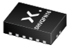
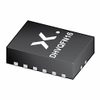
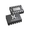
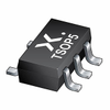
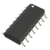
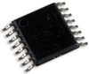
The 74CB3Q3253 is a dual high-bandwidth single-pole, quad-throw FET bus switch. Each switch features a select input (Sn) and an output enable input (nOE). The switch is disabled when the nOEinput is HIGH. An internal charge-pump increases the gate voltage of the NMOS pass transistor. The result is improved RON and RON(flat) performance and the ability to switch 5 V signals when VCC = 3.3 V.
Features and benefits
Wide supply voltage range from 2.3 V to 3.6 V
Overvoltage switching on switch ports:
0 V to 5 V switching with VCC = 2.5 V
0 V to 5 V switching with VCC = 3.3 V
Switch voltage accepts signals up to 5.5 V
4 Ω (typical) ON resistance
3.5 pF (typical) OFF-state capacitance
High bandwidth 0.5 GHz (maximum)
Low input/output capacitance minimizes loading and signal distortion
Fast switching frequency fmax = 20 MHz (maximum)
Low power consumption ICC = 0.4 mA (typical)
Control inputs can be driven by TTL or 5 V/3.3 V CMOS outputs
IOFF supports partial power-down mode operation
Latch-up performance exceeds 100 mA per JESD 78E Class II Level A
ESD protection:
HBM: ANSI/ESDA/JEDEC JS-001 class 2 exceeds 2000 V
CDM: ANSI/ESDA/JEDEC JS-002 class C3 exceeds 1000 V
Specified from -40 °C to +85 °C
Applications
Communication infrastructure
Bus isolation
Memory interleaving
Sensor multiplexing
The 74CB3Q3253 is a dual high-bandwidth single-pole, quad-throw FET bus switch. Each switch features a select input (Sn) and an output enable input (nOE). The switch is disabled when the nOEinput is HIGH. An internal charge-pump increases the gate voltage of the NMOS pass transistor. The result is improved RON and RON(flat) performance and the ability to switch 5 V signals when VCC = 3.3 V.
Features and benefits
- Wide supply voltage range from 2.3 V to 3.6 V
- Overvoltage switching on switch ports:
- 0 V to 5 V switching with VCC = 2.5 V
- 0 V to 5 V switching with VCC = 3.3 V
- Switch voltage accepts signals up to 5.5 V
- 4 Ω (typical) ON resistance
- 3.5 pF (typical) OFF-state capacitance
- High bandwidth 0.5 GHz (maximum)
- Low input/output capacitance minimizes loading and signal distortion
- Fast switching frequency fmax = 20 MHz (maximum)
- Low power consumption ICC = 0.4 mA (typical)
- Control inputs can be driven by TTL or 5 V/3.3 V CMOS outputs
- IOFF supports partial power-down mode operation
- Latch-up performance exceeds 100 mA per JESD 78E Class II Level A
- ESD protection:
- HBM: ANSI/ESDA/JEDEC JS-001 class 2 exceeds 2000 V
- CDM: ANSI/ESDA/JEDEC JS-002 class C3 exceeds 1000 V
- Specified from -40 °C to +85 °C
Applications
- Communication infrastructure
- Bus isolation
- Memory interleaving
- Sensor multiplexing