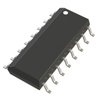
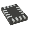
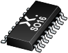
Nexperia B.V. Quad 2-input multiplexer 74AHCT157D-Q100J

Description
The 74AHC/AHCT157-Q100 are high-speed Si-gate CMOS devices and are pin compatible with Low Power Schottky TTL (LSTTL). They are specified in compliance with JEDEC standard no. 7A. The 74AHC/AHCT157-Q100 are quad 2-input multiplexer which select 4 bits of data from two sources under the control of a common data select input (S). The enable input (E) is active LOW. When Eis HIGH, all of the outputs (1Y to 4Y) are forced LOW regardless of all other input conditions. Moving the data from two groups of registers to four common output buses is a common use of the 74AHC/AHCT157-Q100. The state of the common data select input (S) determines the particular register from which the data comes. It can also be used as function generator. The device is useful for implementing highly irregular logic by generating any four of the 16 different functions of two variables with one variable common. The 74AHC/AHCT157-Q100 is logic implementation of a 4-pole, 2-position switch, where the position of the switch is determine by the logic levels applied to S. The logic equations are: 1Y = E× (1I1 × S + 1I0 × S) 2Y = E× (2I1 × S + 2I0 × S) 3Y = E× (3I1 × S + 3I0 × S) 4Y = E× (4I1 × S + 4I0 × S) This product has been qualified to the Automotive Electronics Council (AEC) standard Q100 (Grade 1) and is suitable for use in automotive applications. Features and benefits Automotive product qualification in accordance with AEC-Q100 (Grade 1) Specified from -40 °C to +85 °C and from -40 °C to +125 °C Balanced propagation delays All inputs have a Schmitt-trigger action Inputs accepts voltages higher than VCC Multiple input enable for easy expansion Ideal for memory chip select decoding For 74AHC157-Q100 only: operates with CMOS input levels For 74AHCT157-Q100 only: operates with TTL input levels ESD protection: HBM: ANSI/ESDA/JEDEC JS-001 class 2 exceeds 2000 V CDM: ANSI/ESDA/JEDEC JS-002 class C3 exceeds 1000 V Multiple package options DHVQFN package with Side-Wettable Flanks enabling Automatic Optical Inspection (AOI) of solder joints
Request a Quote Datasheet
Description
The 74AHC/AHCT157-Q100 are high-speed Si-gate CMOS devices and are pin compatible with Low Power Schottky TTL (LSTTL). They are specified in compliance with JEDEC standard no. 7A. The 74AHC/AHCT157-Q100 are quad 2-input multiplexer which select 4 bits of data from two sources under the control of a common data select input (S). The enable input (E) is active LOW. When Eis HIGH, all of the outputs (1Y to 4Y) are forced LOW regardless of all other input conditions. Moving the data from two groups of registers to four common output buses is a common use of the 74AHC/AHCT157-Q100. The state of the common data select input (S) determines the particular register from which the data comes. It can also be used as function generator. The device is useful for implementing highly irregular logic by generating any four of the 16 different functions of two variables with one variable common. The 74AHC/AHCT157-Q100 is logic implementation of a 4-pole, 2-position switch, where the position of the switch is determine by the logic levels applied to S. The logic equations are: 1Y = E× (1I1 × S + 1I0 × S) 2Y = E× (2I1 × S + 2I0 × S) 3Y = E× (3I1 × S + 3I0 × S) 4Y = E× (4I1 × S + 4I0 × S) This product has been qualified to the Automotive Electronics Council (AEC) standard Q100 (Grade 1) and is suitable for use in automotive applications. Features and benefits Automotive product qualification in accordance with AEC-Q100 (Grade 1) Specified from -40 °C to +85 °C and from -40 °C to +125 °C Balanced propagation delays All inputs have a Schmitt-trigger action Inputs accepts voltages higher than VCC Multiple input enable for easy expansion Ideal for memory chip select decoding For 74AHC157-Q100 only: operates with CMOS input levels For 74AHCT157-Q100 only: operates with TTL input levels ESD protection: HBM: ANSI/ESDA/JEDEC JS-001 class 2 exceeds 2000 V CDM: ANSI/ESDA/JEDEC JS-002 class C3 exceeds 1000 V Multiple package options DHVQFN package with Side-Wettable Flanks enabling Automatic Optical Inspection (AOI) of solder joints
Request a Quote Datasheet

Suppliers

Company
Product
Description
Supplier Links
Quad 2-input multiplexer - 74AHCT157D-Q100J - Nexperia B.V.
Nijmegen, Netherlands
Quad 2-input multiplexer
74AHCT157D-Q100J
Quad 2-input multiplexer 74AHCT157D-Q100J
The 74AHC/AHCT157-Q100 are high-speed Si-gate CMOS devices and are pin compatible with Low Power Schottky TTL (LSTTL). They are specified in compliance with JEDEC standard no. 7A. The 74AHC/AHCT157-Q100 are quad 2-input multiplexer which select 4 bits of data from two sources under the control of a common data select input (S). The enable input (E) is active LOW. When Eis HIGH, all of the outputs (1Y to 4Y) are forced LOW regardless of all other input conditions. Moving the data from two groups of registers to four common output buses is a common use of the 74AHC/AHCT157-Q100. The state of the common data select input (S) determines the particular register from which the data comes. It can also be used as function generator. The device is useful for implementing highly irregular logic by generating any four of the 16 different functions of two variables with one variable common. The 74AHC/AHCT157-Q100 is logic implementation of a 4-pole, 2-position switch, where the position of the switch is determine by the logic levels applied to S. The logic equations are: 1Y = E× (1I1 × S + 1I0 × S) 2Y = E× (2I1 × S + 2I0 × S) 3Y = E× (3I1 × S + 3I0 × S) 4Y = E× (4I1 × S + 4I0 × S) This product has been qualified to the Automotive Electronics Council (AEC) standard Q100 (Grade 1) and is suitable for use in automotive applications. Features and benefits Automotive product qualification in accordance with AEC-Q100 (Grade 1) Specified from -40 °C to +85 °C and from -40 °C to +125 °C Balanced propagation delays All inputs have a Schmitt-trigger action Inputs accepts voltages higher than VCC Multiple input enable for easy expansion Ideal for memory chip select decoding For 74AHC157-Q100 only: operates with CMOS input levels For 74AHCT157-Q100 only: operates with TTL input levels ESD protection: HBM: ANSI/ESDA/JEDEC JS-001 class 2 exceeds 2000 V CDM: ANSI/ESDA/JEDEC JS-002 class C3 exceeds 1000 V Multiple package options DHVQFN package with Side-Wettable Flanks enabling Automatic Optical Inspection (AOI) of solder joints

The 74AHC/AHCT157-Q100 are high-speed Si-gate CMOS devices and are pin compatible with Low Power Schottky TTL (LSTTL). They are specified in compliance with JEDEC standard no. 7A.

The 74AHC/AHCT157-Q100 are quad 2-input multiplexer which select 4 bits of data from two sources under the control of a common data select input (S). The enable input (E) is active LOW. When Eis HIGH, all of the outputs (1Y to 4Y) are forced LOW regardless of all other input conditions.

Moving the data from two groups of registers to four common output buses is a common use of the 74AHC/AHCT157-Q100. The state of the common data select input (S) determines the particular register from which the data comes. It can also be used as function generator. The device is useful for implementing highly irregular logic by generating any four of the 16 different functions of two variables with one variable common. The 74AHC/AHCT157-Q100 is logic implementation of a 4-pole, 2-position switch, where the position of the switch is determine by the logic levels applied to S.

The logic equations are:

  • 1Y = E× (1I1 × S + 1I0 × S)
  • 2Y = E× (2I1 × S + 2I0 × S)
  • 3Y = E× (3I1 × S + 3I0 × S)
  • 4Y = E× (4I1 × S + 4I0 × S)

This product has been qualified to the Automotive Electronics Council (AEC) standard Q100 (Grade 1) and is suitable for use in automotive applications.

Features and benefits

  • Automotive product qualification in accordance with AEC-Q100 (Grade 1)
    • Specified from -40 °C to +85 °C and from -40 °C to +125 °C
  • Balanced propagation delays
  • All inputs have a Schmitt-trigger action
  • Inputs accepts voltages higher than VCC
  • Multiple input enable for easy expansion
  • Ideal for memory chip select decoding
  • For 74AHC157-Q100 only: operates with CMOS input levels
  • For 74AHCT157-Q100 only: operates with TTL input levels
  • ESD protection:
    • HBM: ANSI/ESDA/JEDEC JS-001 class 2 exceeds 2000 V
    • CDM: ANSI/ESDA/JEDEC JS-002 class C3 exceeds 1000 V
  • Multiple package options
  • DHVQFN package with Side-Wettable Flanks enabling Automatic Optical Inspection (AOI) of solder joints
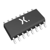
Supplier's Site Datasheet
Integrated Circuits (ICs) - Logic - Signal Switches, Multiplexers, Decoders - 74AHCT157D-Q100J - Shenzhen Shengyu Electronics Technology Limited
Futian, China
Integrated Circuits (ICs) - Logic - Signal Switches, Multiplexers, Decoders
74AHCT157D-Q100J
Integrated Circuits (ICs) - Logic - Signal Switches, Multiplexers, Decoders 74AHCT157D-Q100J
IC MULTIPLEXER 4 X 2:1 16SO

IC MULTIPLEXER 4 X 2:1 16SO

Supplier's Site
Signal Switches, Multiplexers, Decoders - 74AHCT157D-Q100J - Quarktwin Technology Ltd.
Shenzhen, Guangdong, China
Signal Switches, Multiplexers, Decoders
74AHCT157D-Q100J
Signal Switches, Multiplexers, Decoders 74AHCT157D-Q100J
Multiplexer 4 x 2:1 16-SO

Multiplexer 4 x 2:1 16-SO

Buy Now Datasheet

Technical Specifications

  Nexperia B.V. Shenzhen Shengyu Electronics Technology Limited Quarktwin Technology Ltd.
Product Category Logic Multiplexers Logic Multiplexers Logic Multiplexers
Product Number 74AHCT157D-Q100J 74AHCT157D-Q100J 74AHCT157D-Q100J
Product Name Quad 2-input multiplexer Integrated Circuits (ICs) - Logic - Signal Switches, Multiplexers, Decoders Signal Switches, Multiplexers, Decoders
Features ESD Protection
Unlock Full Specs
to access all available technical data

Similar Products