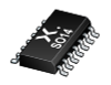
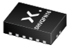
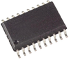
The 74AHC164-Q100; 74AHCT164-Q100 is an 8-bit serial-in/parallel-o
ut shift register. The device features two serial data inputs (DSA and DSB), eight parallel data outputs (Q0 to Q7). Data is entered serially through DSA or DSB and either input can be used as an active HIGH enable for data entry through the other input. Data is shifted on the LOW-to-HIGH transitions of the clock (CP) input. A LOW on the master reset input (MR) clears the register and forces all outputs LOW, independently of other inputs. Inputs are overvoltage tolerant. This feature allows the use of these devices as translators in mixed voltage environments.
This product has been qualified to the Automotive Electronics Council (AEC) standard Q100 (Grade 1) and is suitable for use in automotive applications.
Features and benefits
Automotive product qualification in accordance with AEC-Q100 (Grade 1)
Specified from -40 °C to +85 °C and from -40 °C to +125 °C
Wide supply voltage range from 2.0 V to 5.5 V
Overvoltage tolerant inputs to 5.5 V
High noise immunity
CMOS low power dissipation
Balanced propagation delays
All inputs have Schmitt-trigger actions
Input levels:
For 74AHC164-Q100: CMOS level
For 74AHCT164-Q100: TTL level
Latch-up performance exceeds 100 mA per JESD 78 Class II Level A
ESD protection:
HBM: ANSI/ESDA/JEDEC JS-001 class 2 exceeds 2000 V
CDM: ANSI/ESDA/JEDEC JS-002 class C3 exceeds 1000 V
Multiple package options
DHVQFN package with Side-Wettable Flanks enabling Automatic Optical Inspection (AOI) of solder joints
The 74AHC164-Q100; 74AHCT164-Q100 is an 8-bit serial-in/parallel-out shift register. The device features two serial data inputs (DSA and DSB), eight parallel data outputs (Q0 to Q7). Data is entered serially through DSA or DSB and either input can be used as an active HIGH enable for data entry through the other input. Data is shifted on the LOW-to-HIGH transitions of the clock (CP) input. A LOW on the master reset input (MR) clears the register and forces all outputs LOW, independently of other inputs. Inputs are overvoltage tolerant. This feature allows the use of these devices as translators in mixed voltage environments.
This product has been qualified to the Automotive Electronics Council (AEC) standard Q100 (Grade 1) and is suitable for use in automotive applications.
Features and benefits
- Automotive product qualification in accordance with AEC-Q100 (Grade 1)
- Specified from -40 °C to +85 °C and from -40 °C to +125 °C
- Wide supply voltage range from 2.0 V to 5.5 V
- Overvoltage tolerant inputs to 5.5 V
- High noise immunity
- CMOS low power dissipation
- Balanced propagation delays
- All inputs have Schmitt-trigger actions
- Input levels:
- For 74AHC164-Q100: CMOS level
- For 74AHCT164-Q100: TTL level
- Latch-up performance exceeds 100 mA per JESD 78 Class II Level A
- ESD protection:
- HBM: ANSI/ESDA/JEDEC JS-001 class 2 exceeds 2000 V
- CDM: ANSI/ESDA/JEDEC JS-002 class C3 exceeds 1000 V
- Multiple package options
- DHVQFN package with Side-Wettable Flanks enabling Automatic Optical Inspection (AOI) of solder joints