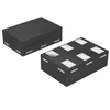
The BGA9V1MN9 is a low noise amplifier for LTE and 5G which covers a wide frequency range from 3.3 GHz to 4.2 GHz. The LNA provides up to 21.0 dB gain and 0.75 dB noise figure at a current consumption of 5.8 mA in the application configuration described in Chapter 7. With the Gain Step feature the gain and linearity can be adjusted to increase the system dynamic range and to accommodate to changing interference scenarios.
The BGA9V1MN9 supports ultra-low bypass current of 2 µA and 1.2 V operating voltage to reduce power consumption. It operates from 1.1 V to 2.0 V supply voltage over temperature. The compact9 pin TSNP-9 package with the dimension of 1.1 x 1.1 mm helps to save space on the PCB.
Summary of Features
Power gain: 21.0 dB
Low noise figure: 0.75 dB
Low current consumption: 5.8 mA
Frequency range from 3.3 to 4.2 GHz
Supply voltage: 1.1 to 2.0 V
Integrated MIPI RFFE interface operating in 1.65 to 1.95 V voltage range
Software programmable MIPI RFFE USID
USID select pin
Small form factor 1.1 mm x 1.1 mm
High EMI robustness
RoHS and WEEE compliant package
Potential Applications
LTE / 5G Smartphones
Applications
Mobile devices and smartphones
Designers who used this product also designed with
BGSA149MN10 | Antenna tuners
BGSA14M2N10 | Antenna tuners
BGSA147ML10 | Antenna tuners
BGSA149M2N10 | Antenna tuners
BGS12P2L6 | RF Switches
BGS14WMA9 | RF Switches
BGM687U50 | 4G/5G MIPI LNA and LNA Bank
BGS14M8U9 | RF Switches
BGSX22G5A10 | Antenna cross switches
BGS12WN6 | RF Switches
BGSA149MN10 | Antenna tuners
BGSA14M2N10 | Antenna tuners
BGSA147ML10 | Antenna tuners
BGSA149M2N10 | Antenna tuners
BGS12P2L6 | RF Switches
BGS14WMA9 | RF Switches
BGM687U50 | 4G/5G MIPI LNA and LNA Bank
BGS14M8U9 | RF Switches
1 2 3
The BGA9V1MN9 is a low noise amplifier for LTE and 5G which covers a wide frequency range from 3.3 GHz to 4.2 GHz. The LNA provides up to 21.0 dB gain and 0.75 dB noise figure at a current consumption of 5.8 mA in the application configuration described in Chapter 7. With the Gain Step feature the gain and linearity can be adjusted to increase the system dynamic range and to accommodate to changing interference scenarios.
The BGA9V1MN9 supports ultra-low bypass current of 2 µA and 1.2 V operating voltage to reduce power consumption. It operates from 1.1 V to 2.0 V supply voltage over temperature. The compact9 pin TSNP-9 package with the dimension of 1.1 x 1.1 mm helps to save space on the PCB.
Summary of Features
- Power gain: 21.0 dB
- Low noise figure: 0.75 dB
- Low current consumption: 5.8 mA
- Frequency range from 3.3 to 4.2 GHz
- Supply voltage: 1.1 to 2.0 V
- Integrated MIPI RFFE interface operating in 1.65 to 1.95 V voltage range
- Software programmable MIPI RFFE USID
- USID select pin
- Small form factor 1.1 mm x 1.1 mm
- High EMI robustness
- RoHS and WEEE compliant package
Potential Applications
LTE / 5G Smartphones
Applications
- Mobile devices and smartphones
Designers who used this product also designed with
- BGSA149MN10 |
Antenna tuners
- BGSA14M2N10 |
Antenna tuners
- BGSA147ML10 |
Antenna tuners
- BGSA149M2N10 |
Antenna tuners
- BGS12P2L6 |
RF Switches
- BGS14WMA9 |
RF Switches
- BGM687U50 |
4G/5G MIPI LNA and LNA Bank
- BGS14M8U9 |
RF Switches
- BGSX22G5A10 |
Antenna cross switches
- BGS12WN6 |
RF Switches
- BGSA149MN10 |
Antenna tuners
- BGSA14M2N10 |
Antenna tuners
- BGSA147ML10 |
Antenna tuners
- BGSA149M2N10 |
Antenna tuners
- BGS12P2L6 |
RF Switches
- BGS14WMA9 |
RF Switches
- BGM687U50 |
4G/5G MIPI LNA and LNA Bank
- BGS14M8U9 |
RF Switches
1
2
3